Rooted in China · Global discrete semiconductor supportGlobal semiconductor support

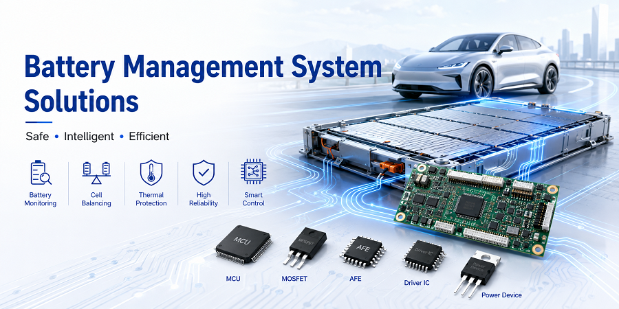
Battery Management System Solutions

Low-loss charge and discharge bus switching solutions for protected, efficient and serviceable multi-cell battery packs.

Battery management system application

Protected bidirectional power flow for rechargeable battery packs

A battery management system must connect the cell stack to the charger and system load with very low loss while opening the power path immediately when an unsafe condition is detected. The bus charge and discharge switch normally uses back-to-back MOSFETs controlled by the BMS monitor or protection controller. This arrangement supports independent charge and discharge control, reverse-current blocking, precharge coordination and rapid isolation during overvoltage, undervoltage, overcurrent, short-circuit or thermal faults. Device selection must balance voltage margin, low RDS(on), gate charge, pulse-current capability, safe operating area and package thermal performance.

Key advantages

  • Low charge-path resistance
  • Low discharge-path resistance
  • Independent CHG and DSG control
  • Reverse-current blocking
  • Fast short-circuit isolation
  • High pulse-current capability
  • Strong safe operating area
  • Precharge coordination
  • Low standby consumption
  • Thermal-aware protection
  • Scalable pack voltage
  • Reliable fault containment

Battery management system architecture and product mapping

Battery Management System Architecture

Cell-stack supervision, protected bidirectional pack switching, fault isolation, sensing and host communication.

Battery Management System Solutions Editable two-to-one SVG block diagram for a battery management system. The interactive MOT-supported module is the Bus Charge and Discharge Switch. BATTERY MANAGEMENT SYSTEM SOLUTIONS CELL MONITORING, PROTECTION & BIDIRECTIONAL PACK POWER PATH Cell Stack, Sensing & BMS Control Multi-Cell Battery Stack Cell taps · pack voltage · temperature points AFE Monitor Protection Controller Voltage · current · temperature SOC / SOH · balancing · diagnostics CELL MEASUREMENT · BALANCE CONTROL · PACK DIAGNOSTICS Bus Charge & Discharge Switch CHG DSG Back-to-back MOSFETs · reverse-current blocking · fast fault isolation PACK BUS BIDIRECTIONAL CURRENT Charger Port System Load CHG / DSG GATE CONTROL · OVP · UVP · OCP · SCP · OTP The protected bus switch connects the pack during normal operation and isolates the charger or load when the BMS detects an unsafe condition. Filled block: MOT supported device candidates Outline block: necessary system function MOT Semiconductor Solutions
Tip: Select a block in the diagram or choose a module from the list. On mobile, swipe horizontally to view the full diagram.

Explore the battery-management architecture through the interactive block diagram. Select Bus Charge & Discharge Switch to review its electrical role, protection priorities and placeholder MOT device mapping.

About the solution

Back-to-back MOSFET control for bidirectional current flow and rapid fault isolation

The charge and discharge switch is placed between the cell stack and the external pack terminals. The BMS monitor controls separate CHG and DSG gates so the pack can accept charging current, deliver load current, block reverse current or isolate either direction independently. During an overvoltage, undervoltage, overcurrent, short-circuit or thermal event, the controller removes gate drive and forces the power path into a defined safe state. Low resistance, strong pulse capability and predictable gate behavior are therefore central design priorities.

Adaptable to mobility, tools, storage, robotics and industrial battery systems

The same protected bus-switch concept is used in portable energy-storage products, e-bikes and scooters, power tools, garden equipment, robotics, UPS battery modules, industrial instruments and other rechargeable systems. Pack voltage, continuous current, peak current, cell chemistry, connector behavior, precharge sequence, short-circuit threshold and thermal environment determine the required MOSFET voltage rating, parallel-device count, package and driver strategy.

Power devices and drivers selected around conduction loss, SOA and fault response

Low-RDS(on) N-channel MOSFETs, dual back-to-back MOSFET packages, high-side gate drivers, fast battery-protection controllers, current-sense interfaces, transient suppressors and temperature-monitoring devices form the semiconductor platform for a robust charge and discharge path. The final selection should be validated against normal operating current, startup and regenerative pulses, short-circuit energy, board copper area and worst-case junction temperature.

Back-to-back MOSFET control for bidirectional current flow and rapid fault isolation

The charge and discharge switch is placed between the cell stack and the external pack terminals. The BMS monitor controls separate CHG and DSG gates so the pack can accept charging current, deliver load current, block reverse current or isolate either direction independently. During an overvoltage, undervoltage, overcurrent, short-circuit or thermal event, the controller removes gate drive and forces the power path into a defined safe state. Low resistance, strong pulse capability and predictable gate behavior are therefore central design priorities.

Adaptable to mobility, tools, storage, robotics and industrial battery systems

The same protected bus-switch concept is used in portable energy-storage products, e-bikes and scooters, power tools, garden equipment, robotics, UPS battery modules, industrial instruments and other rechargeable systems. Pack voltage, continuous current, peak current, cell chemistry, connector behavior, precharge sequence, short-circuit threshold and thermal environment determine the required MOSFET voltage rating, parallel-device count, package and driver strategy.

Power devices and drivers selected around conduction loss, SOA and fault response

Low-RDS(on) N-channel MOSFETs, dual back-to-back MOSFET packages, high-side gate drivers, fast battery-protection controllers, current-sense interfaces, transient suppressors and temperature-monitoring devices form the semiconductor platform for a robust charge and discharge path. The final selection should be validated against normal operating current, startup and regenerative pulses, short-circuit energy, board copper area and worst-case junction temperature.

Contact our engineering team

Talk to Engineering Sales

Tell us your operating conditions and volume plan.

Share your target application, electrical requirements, package preference and estimated quantity. Our field application engineers will follow up with the right battery-charging devices and reference designs for your project.

  • Response from a dedicated FAE within 1 business day
  • Free samples available for qualified design-ins
  • NDA-protected review for early-stage projects
Contact Form