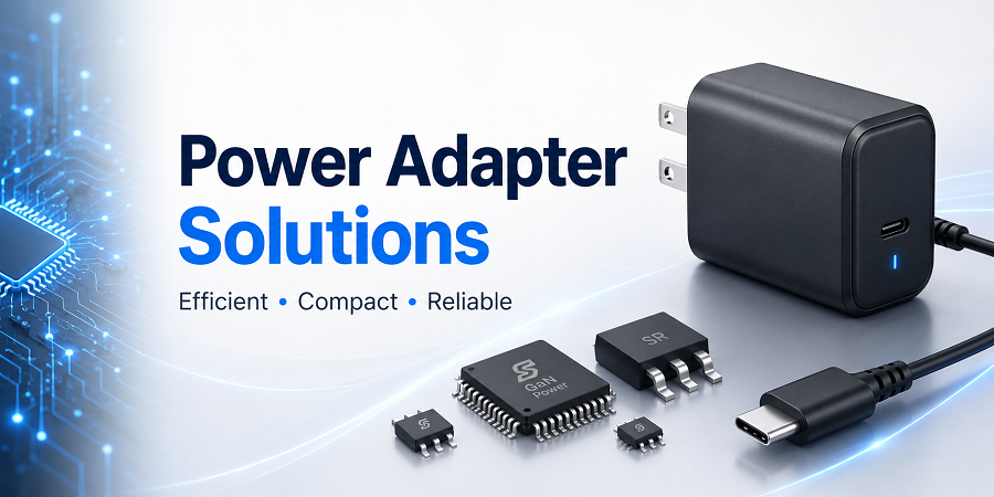
Compact, high-efficiency AC/DC power conversion for USB-C chargers, wall adapters, external power supplies and embedded auxiliary-power applications.
High-density, protected AC/DC conversion for modern power adapters
Power adapters convert a universal AC input into a safe, isolated and tightly regulated DC output for notebooks, mobile devices, networking equipment, consumer electronics and industrial systems. The architecture combines input protection and rectification, active PFC where required, an isolated high-voltage DC/DC primary stage, low-loss synchronous rectification and a main controller that coordinates CC/CV regulation, startup, thermal management and fault protection.
Key advantages
Universal AC input
High power factor
High conversion efficiency
Compact power density
Low no-load power
Accurate CC/CV regulation
Low output ripple
Fast transient response
Reinforced isolation support
Surge and brownout robustness
Coordinated fault protection
Scalable output power
Power adapter architecture and product mapping
Power Adapter Architecture
AC input protection and rectification, active PFC, isolated high-voltage DC/DC conversion, synchronous rectification, output filtering and coordinated CC/CV control.
Tip: Select a block in the diagram or choose a module from the list. On mobile, swipe horizontally to view the full diagram.
Explore the power-adapter architecture through an interactive image map. Select PFC, the isolated high-voltage primary stage, synchronous rectification, or the main controller to review its design role and recommended MOT device categories.
About the solution
High-density isolated conversion with coordinated efficiency and protection
The solution combines universal-input protection and rectification, active power-factor correction where required, an isolated flyback, active-clamp flyback or resonant primary stage, low-loss synchronous rectification and closed-loop CC/CV control. The resulting architecture supports predictable startup, high efficiency, low standby power and stable regulation across line, load and output-voltage transitions.
Scalable for USB-C chargers, wall adapters and external power supplies
The same functional platform can be adapted for smartphone and tablet chargers, notebook adapters, networking equipment, set-top boxes, monitors, smart-home products, portable medical equipment and industrial control systems. Topology, semiconductor voltage rating, thermal design and protocol interface can be scaled to meet the required output power, enclosure size and safety standard.
Device categories aligned with every critical conversion stage
PFC controllers and switches, high-voltage super-junction or wide-bandgap primary devices, isolated and non-isolated gate drivers, low-resistance secondary MOSFETs, synchronous-rectifier controllers, precision feedback devices and supervisory controllers provide a practical component platform for compact, efficient and reliable adapter designs.
High-density isolated conversion with coordinated efficiency and protection
The solution combines universal-input protection and rectification, active power-factor correction where required, an isolated flyback, active-clamp flyback or resonant primary stage, low-loss synchronous rectification and closed-loop CC/CV control. The resulting architecture supports predictable startup, high efficiency, low standby power and stable regulation across line, load and output-voltage transitions.
Scalable for USB-C chargers, wall adapters and external power supplies
The same functional platform can be adapted for smartphone and tablet chargers, notebook adapters, networking equipment, set-top boxes, monitors, smart-home products, portable medical equipment and industrial control systems. Topology, semiconductor voltage rating, thermal design and protocol interface can be scaled to meet the required output power, enclosure size and safety standard.
Device categories aligned with every critical conversion stage
PFC controllers and switches, high-voltage super-junction or wide-bandgap primary devices, isolated and non-isolated gate drivers, low-resistance secondary MOSFETs, synchronous-rectifier controllers, precision feedback devices and supervisory controllers provide a practical component platform for compact, efficient and reliable adapter designs.
Contact our engineering team
Talk to Engineering Sales
Tell us your operating conditions and volume plan.
Share your target application, electrical requirements, package preference and estimated quantity. Our field application engineers will follow up with the right battery-charging devices and reference designs for your project.
Response from a dedicated FAE within 1 business day