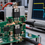
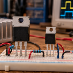
In a hot-swap circuit, the pass MOSFET is intentionally held between fully off and fully enhanced while the downstream capacitance charges. During this interval it can support substantial drain voltage and current at the same time. That operating condition is very different from normal switching, and the familiar current rating or room-temperature on-resistance does not describe it. The safe operating area, or SOA, is the correct starting point.
Translate the system event into device stress
Begin with the worst credible input voltage, load capacitance, programmed current limit, power limit, and fault timer. For a simple constant-current startup, the MOSFET drain voltage falls as the output capacitor charges. A power-limiting controller produces a different trajectory because current changes with drain voltage. Output short circuit, insertion into a charged bus, and restart into a partially charged load can each create a separate worst case.
Plot or calculate the simultaneous values of VDS and ID over time. The important question is not only the peak power. The pulse duration and the shape of the stress determine how heat spreads through the die and package. Compare several points along the trajectory with the appropriate SOA pulse-duration boundary.
Read the graph conservatively
Datasheet SOA graphs usually assume a defined mounting-base or case temperature and a single pulse. They may show boundaries caused by maximum current, on-resistance, power dissipation, or electrothermal instability. Interpolating between curves can be useful for screening, but it should not replace a transient thermal calculation or hardware validation near the limit.
- Use the curve for a pulse duration at least as long as the actual stress.
- Derate when the initial junction or mounting-base temperature is above the graph condition.
- Include controller tolerances that raise current limit or extend the fault timer.
- Check minimum and maximum input voltage because the worst combination may change.
- Do not assume paralleled MOSFETs share linear-mode current equally.
Account for temperature before the event
A hot-swap MOSFET rarely starts at 25 °C in a real system. Nearby power converters, limited airflow, and repeated insertions can raise its initial junction temperature. Estimate the pre-event temperature from steady-state conduction loss and the board thermal path. Then add the transient temperature rise associated with the startup or fault waveform. Keep margin below the maximum junction temperature and below any manufacturer-specific linear-mode limit.
When several MOSFETs are placed in parallel, small threshold differences can cause one device to enter conduction first. In linear mode, local heating can worsen the imbalance. Individual gate resistors, close thermal coupling, matched layout, and validated sharing are essential; simply dividing the calculated power by the number of devices is not enough.
Validate the controller and MOSFET together
Use a current probe and differential voltage probe to capture the actual event. Integrate instantaneous power to understand energy, but also compare the measured VDS-ID trajectory with SOA. Test startup, output short, timer expiration, retry behavior, brownout, and rapid power cycling. Measure case or board temperature and use a calibrated thermal model to estimate junction temperature.
A robust selection process leaves margin for part variation, hot ambient, aging airflow, and abnormal but specified events. The best hot-swap MOSFET is not necessarily the device with the lowest on-resistance; it is the device that combines acceptable conduction loss with documented, repeatable linear-mode capability.
Technical reference: Texas Instruments, Robust Hot Swap Design.