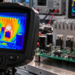
A power MOSFET’s electrical loss becomes heat at the junction. Whether the design is reliable depends on the complete path from silicon to package, PCB copper, thermal vias, heatsink or chassis, and ambient air. A thermal-resistance number copied from a datasheet is useful only when its boundary condition resembles the real assembly.
Begin with realistic power loss
Calculate conduction loss with on-resistance at the expected junction temperature, not only the 25 °C value. Add switching energy at the actual voltage, current, gate drive, and frequency. Include body-diode or reverse-conduction loss, gate-drive loss when relevant to the package temperature, and any linear-mode or avalanche events that contribute meaningful average heating.
Because on-resistance rises with temperature, conduction loss and junction temperature are coupled. Iterate the calculation until the assumed and calculated temperature agree.
Read thermal metrics by boundary condition
Junction-to-ambient resistance is highly dependent on PCB area, layer count, copper thickness, airflow, orientation, and nearby heat sources. Junction-to-case or junction-to-mounting-base values are more portable only when that surface is held at a known temperature. Transient thermal impedance describes short pulses before the entire assembly reaches steady state.
- Use the datasheet board description as a reference, not a universal constant.
- Separate vertical heat flow through the package from lateral spreading in copper.
- Include thermal-interface material resistance and contact pressure for a heatsink.
- Model neighboring devices that share the same copper or enclosure.
Use copper and vias intentionally
For bottom-cooled packages, connect the thermal pad to a compact via array and spreading planes on internal or opposite layers. Keep vias close enough to the heat source to be useful, while meeting solder-voiding and assembly rules. For top-cooled packages, provide a controlled interface to a heatsink or chassis and manage electrical isolation if the exposed surface is not at a safe potential.
More copper does not always produce a proportional improvement. Once heat has spread across the useful board area, convection and the enclosure may dominate. Large switch-node copper can also increase parasitic capacitance and EMI, so electrical and thermal layout must be solved together.
Measure with a calibrated method
An infrared image shows surface temperature, which may be significantly below junction temperature. Emissivity differences on copper, solder, mold compound, and metal clips can distort readings. A thermocouple adds thermal mass and measures only its attachment point. Both methods are valuable when correlated to a calibrated junction-temperature estimate.
Possible approaches include a temperature-sensitive electrical parameter, a validated compact thermal model, or a power-step calibration that relates case or board temperature to junction temperature. Capture ambient and airflow conditions, and allow the assembly to reach steady state when evaluating continuous operation.
Validate abnormal and transient states
Run maximum continuous load, overload timer, startup, stall, short circuit, and burst operation as applicable. Use transient thermal impedance for short events and cumulative heating for repeated pulses. Confirm that protection acts before the junction crosses the derated limit, including sensor delay and device tolerances.
A good thermal design is visible in the release documentation: loss assumptions, boundary conditions, board construction, interfaces, airflow, measured temperatures, and junction estimate all connect. That chain makes the result portable when the package, board, or enclosure changes.
Technical reference: Nexperia, LFPAK MOSFET thermal design guide.