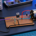
How do you use a MOSFET? Choose the correct polarity and voltage class, connect it as a low-side or high-side switch, drive the gate relative to the source, provide a defined off state, protect the device from inductive and voltage transients, and verify electrical and thermal limits. The MOSFET then lets a low-power control signal switch or regulate a larger current.
The most common beginner application is an enhancement-mode N-channel MOSFET used as a low-side switch for a DC load. The same design principles extend to PWM, converters, motor drives, battery protection, and power-path control.
Understand the three main terminals
- Gate: the voltage-controlled terminal. The driver charges and discharges its capacitance.
- Drain: one end of the controlled current path.
- Source: the other end of the path and the reference point for gate voltage.
The important control quantity is VGS, not gate voltage relative to an arbitrary board ground. An N-channel device turns on when its gate is sufficiently positive relative to its source. A P-channel device turns on when its gate is sufficiently negative relative to its source.
Choose the MOSFET type
| Device | Normal control | Common use |
|---|---|---|
| N-channel enhancement MOSFET | Positive VGS turns it on | Low-side switching, converters, bridge stages |
| P-channel enhancement MOSFET | Negative VGS turns it on | Simple high-side switching at modest power |
| Depletion-mode MOSFET | Normally on at VGS = 0 V | Current sources, startup and specialized analog circuits |
N-channel power MOSFETs normally provide lower on-resistance for a given size and voltage rating. P-channel devices can simplify a high-side circuit but often trade efficiency for simpler drive.
Use an N-channel MOSFET as a low-side switch
Connect the load between the positive supply and drain. Connect source to the power return. Drive the gate through a small series resistor and add a gate-to-source pull-down resistor. The controller and MOSFET source must share a suitable reference unless an isolated driver is used.
- The pull-down keeps the gate near source when the controller starts or is disconnected.
- A high controller output charges the gate and raises VGS.
- The channel turns on and current flows through the load and MOSFET.
- A low output removes gate charge and turns the device off.
This arrangement is simple and efficient, but the load remains connected to the positive supply. If the application requires the load to be referenced to ground, a high-side switch may be more suitable.
Choose voltage and current ratings
Select VDSS above the highest drain-to-source voltage, including input tolerance, inductive overshoot, ringing, load dump, and abnormal conditions. The required margin depends on the environment and protection strategy.
Do not select from the headline current rating alone. Package leads, PCB copper, thermal resistance, and junction temperature usually limit usable continuous current. Calculate loss and temperature for the actual duty cycle.
Use the correct gate voltage
VGS(th) is the voltage at which a small test current begins to flow. It is not the full-on voltage. A MOSFET with a 2 V threshold may still have excessive resistance when driven by a 3.3 V controller.
For direct logic drive, choose a logic-level MOSFET with guaranteed RDS(on) at the available gate voltage. If the datasheet specifies resistance only at 10 V, assume a low-voltage microcontroller cannot fully enhance it unless additional curves and testing prove otherwise.
Add the gate components
Series gate resistor
A resistor between driver and gate limits peak current, damps ringing, and controls switching speed. A larger value can reduce EMI and overshoot but increases switching loss. The correct value depends on driver impedance, gate charge, layout inductance, and switching frequency.
Gate-to-source pull resistor
A pull-down for N-channel or pull-up for P-channel devices defines the off state while the controller pin is floating. Values from several kilohms to hundreds of kilohms are common, but the design must account for leakage, noise, dV/dt coupling, and startup timing.
Gate protection
Keep VGS within its absolute maximum rating. A gate-source Zener or dedicated clamp can protect against ringing in harsh circuits. Place it close to the device and confirm that it does not interfere with normal drive.
Handle inductive loads correctly
Motors, solenoids, relays, transformers, and long wiring store magnetic energy. Current cannot stop instantly when the MOSFET turns off. Provide a path using a flyback diode, TVS diode, active clamp, snubber, synchronous switch, or appropriate converter topology.
A simple flyback diode across a DC coil has its cathode at the positive supply and anode at the MOSFET drain. It clamps voltage but may slow current decay. A higher-voltage clamp releases energy faster and must be rated for the repeated pulse energy.
Estimate conduction loss
For a fully enhanced switch, approximate conduction loss as IRMS2 × RDS(on). Use resistance at the available gate voltage and expected junction temperature. RDS(on) can increase substantially as the device heats.
For example, a 5 A RMS current through 30 mΩ produces about 0.75 W before temperature correction. The package, PCB, airflow, and ambient conditions must remove that heat while keeping the junction below its limit.
Estimate switching loss
During a transition, the MOSFET temporarily supports voltage while carrying current. A first estimate for hard-switching overlap is 0.5 × VDS × ID × (tr + tf) × fSW. Real loss also includes nonlinear capacitance, diode recovery, parasitic inductance, and waveform shape.
Gate-drive power is approximately Qg × Vdrive × fSW. At low switching frequency this may be small. At high frequency, total gate charge and Miller charge strongly affect the required driver.
Decide whether a gate driver is needed
A microcontroller may directly drive a small logic-level MOSFET at low frequency. Use a dedicated driver when gate charge is large, frequency is high, transitions must be controlled, source voltage moves, isolation is required, or rapid fault shutdown is important.
A driver provides higher source and sink current than most logic pins. It can also add undervoltage lockout, Miller clamping, dead-time control, desaturation or overcurrent response, and isolated level shifting.
Use a P-channel MOSFET for simple high-side control
Connect source to the positive supply and drain to the load. A gate-to-source pull-up keeps the device off. Pulling the gate lower turns it on. If supply voltage exceeds the controller rating, use a transistor or driver between the logic signal and gate.
Limit negative VGS so it does not exceed the gate rating. At higher current, an N-channel high-side MOSFET with a bootstrap, charge-pump, or isolated driver usually provides better efficiency.
Use MOSFETs for PWM
Pulse-width modulation changes the fraction of time the device is on. It controls average power in heaters, LEDs, fans, solenoids, and motors. Choose a PWM frequency that balances audible noise, current ripple, control response, switching loss, and EMI.
Measure the actual gate and drain waveforms. A MOSFET that works for occasional on-off control may overheat when switched thousands of times per second by a weak driver.
Understand the body diode
A discrete power MOSFET contains an intrinsic body diode. It can conduct reverse current when the channel is off. When the channel is on, it can normally carry current in either direction, subject to ratings.
One MOSFET cannot block current in both directions while off because the body diode remains. Battery disconnects and bidirectional load switches often use two back-to-back MOSFETs with opposing body diodes.
Layout the circuit as part of the design
- Keep the high-current switching loop short and wide.
- Place local decoupling close to the MOSFET and commutation path.
- Keep gate and driver-return traces short.
- Separate sensitive control signals from the switching node.
- Use adequate copper area, vias, and heatsinking for thermal performance.
- Consider a Kelvin-source connection when source inductance affects gate drive.
Practical design checklist
- Define supply voltage, load current, duty cycle, switching frequency, and ambient temperature.
- Select polarity and low-side or high-side arrangement.
- Choose VDSS margin and verify hot RDS(on).
- Confirm gate drive and maximum VGS.
- Add gate resistor, pull resistor, and protection.
- Provide an inductive-current path where required.
- Estimate conduction, switching, diode, and gate-drive losses.
- Design PCB current loops and thermal path.
- Measure VGS, VDS, current, temperature, and EMI on the prototype.
Common mistakes
- Using threshold voltage as the required drive voltage
- Leaving the gate floating
- Forgetting the controller and source reference
- Omitting the flyback path for an inductive load
- Using room-temperature RDS(on) in the thermal calculation
- Choosing only the lowest resistance and ignoring charge or capacitance
- Driving a large gate directly at high frequency
- Ignoring drain overshoot and source inductance
Frequently asked questions
Can I connect a MOSFET gate directly to 5 V?
Only if the voltage stays within the gate rating and the MOSFET has suitable on-resistance at 5 V. Add a defined pull resistor and consider a series gate resistor. High-frequency or high-power operation may require a driver.
Can a MOSFET replace a relay?
It can switch DC rapidly and silently, but it does not automatically provide galvanic isolation or bidirectional AC blocking. Choose the topology and protection for the load and safety requirements.
Why does my MOSFET get hot?
Common causes are insufficient gate voltage, excessive RMS current, high hot resistance, slow switching, high frequency, body-diode loss, linear operation, and inadequate cooling.
Summary
Using a MOSFET successfully requires more than connecting a logic signal to the gate. Select the correct device, drive VGS properly, define the off state, control inductive energy, calculate loss, design the layout and thermal path, and verify real waveforms. Treat the MOSFET, gate driver, load, and switching loop as one system.