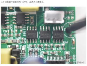
Technical code behind model
The GaN package model uses the " three-part code rule " to pass technical parameters accurately by combining letters and numbers.
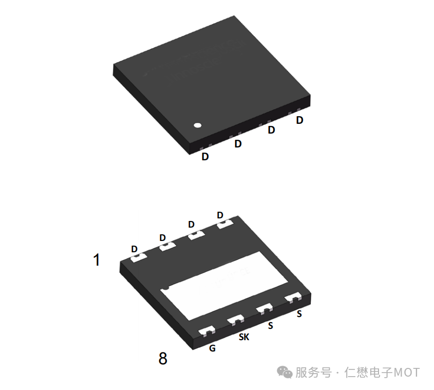
Example model: MOTGE65R190Q
Prefixing technical route
– GE: E-mode nitrogen
– GD: D-mode nitrogen oxides
Technical difference: E-mode devices need not have a negative break and drive circuits are simpler; D-mode needs a combination of drive IC to achieve a permanent closure.
2. Pressure proofing
-65: 650V piercing voltage (actual test value 700V)
-70: 700V piercing voltage (fitting 800V bus system)
3. Controlling electrical resistance precision
-R190: 25 °C at R<sub>DS(on)</sub>=190m
– Test: JEDEC JS-709-1A (pulse method)
4. Seal codes
-Q: DFN8 x 8 (sized 8mm x 8mm, supporting double-sided heat)
-G: DFN5 x 6 (5mm x 6mm, compact design)
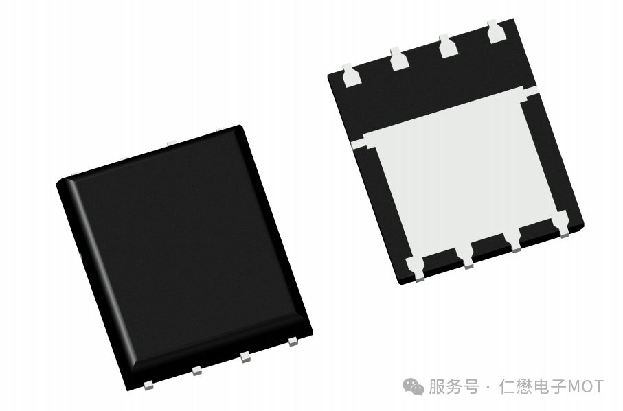
Product matrix versus performance
Type | Type | Stress (V) | R<sub>DS(on)</ sub>(m) < Seal Qsub>g</sub> (nC)
| MOTGE65R190Q |E-mode |650|190 DDFN8x8 8. 8. 5
| MOTGD65R110Q | D-mode | 650 | 110 D DFN5 x 6 | 6. 2
| MOOTGE70R350G | E-mode | 700 | 350 | DFN5 x 6 | 12. 8

Interpretation of key parameters
E-mode Low Qg Advantage: Qg of MoTGE65R190Q only 8. 5nC supports 500kHz HF switches
D-mode ultra-low internal barrier: R<sub>DS(on)</sub> of MOTGD65R110Q is as low as 110 m and lead losses are 60% lower than Silicon MOS

Right away, contact the sales to get the Ingien GaN Handbook.