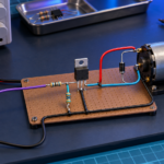
How does a MOSFET transistor work in a real circuit? Gate-to-source voltage creates a conductive channel between drain and source. The controller charges the gate to turn that channel on and removes the charge to turn it off. The load, supply, gate driver, parasitic inductance, body diode, and thermal path determine what happens beyond that ideal description.
A low-side N-channel switch is the clearest practical example. It can control a lamp, heater, solenoid, fan, relay coil, or another DC load from a microcontroller or control IC.
A basic N-channel low-side switch
The circuit connects the positive supply to the load, the load to the MOSFET drain, and the MOSFET source to ground. A control signal drives the gate through a small series resistor. A gate-to-source pull-down resistor keeps the device off when the controller is disconnected or starting.
If the load is inductive, a flyback path is placed across the load or implemented with another switch or clamp. The power ground and signal ground must be connected intentionally so the controller produces the expected VGS.
What happens when the MOSFET is off?
- The pull-down holds the gate near the source potential.
- VGS is approximately zero, so the enhancement-mode channel is absent.
- The load current is near zero except for leakage and any alternate path.
- The drain rises toward the load supply because the off MOSFET blocks the applied voltage.
- The MOSFET’s drain-to-source capacitance stores charge at that voltage.
The selected VDSS rating must cover the supply maximum plus turn-off overshoot and ringing. A 12 V nominal system can experience much higher transients, especially with inductive wiring or automotive supply conditions.
What happens during turn-on?
The controller or driver sources current into the gate. VGS rises until the channel begins to form near threshold. As gate voltage continues upward, drain current increases to the load current and VDS falls. The gate then passes through the Miller plateau while the drain voltage changes.
After the transition, the driver brings VGS to its final value. The MOSFET operates in the ohmic region and its voltage drop is approximately load current multiplied by RDS(on). The resistance used in this calculation must correspond to the actual gate voltage and expected junction temperature.
Why a logic signal may not be enough
A microcontroller output marked high may be 1.8 V, 3.3 V, or 5 V. A MOSFET datasheet may list a threshold between 1 V and 4 V, but threshold is measured at a small current. It does not guarantee low resistance at the load current.
For direct microcontroller drive, choose a logic-level MOSFET with guaranteed RDS(on) at the available gate voltage. Also check whether the microcontroller pin can move the total gate charge quickly enough. A device can be fully enhanced eventually yet spend too long in a high-loss transition at the required PWM frequency.
What the two gate resistors do
Series gate resistor
The series resistor limits peak gate current and works with driver resistance and parasitic inductance to control ringing. Increasing resistance slows drain-voltage and current transitions, which can reduce EMI and overshoot but increase switching loss. Separate turn-on and turn-off paths can be created with a diode and two resistors when asymmetric speeds are useful.
Gate-to-source pull resistor
The pull-down keeps an N-channel MOSFET off when the driver output is high impedance. It must be low enough to overcome leakage and capacitive coupling but high enough not to waste excessive control current. Common values span several kilohms to hundreds of kilohms, but the correct value depends on noise, dV/dt, startup timing, and driver behavior.
How an inductive load changes turn-off
Current in an inductor cannot change instantly. When the MOSFET turns off, the load current forces the drain voltage upward until another path conducts. Without a controlled path, the drain may rise into avalanche or exceed the MOSFET rating.
A flyback diode across a DC coil gives current a safe path. The diode clamps voltage close to the supply, which protects the switch but releases stored energy slowly. A TVS diode, Zener clamp, active clamp, or higher-voltage recirculation path can speed current decay when the load requires a faster release. The selected clamp must handle the energy and repetition rate.
A practical 12 V solenoid example
Assume a 12 V solenoid draws 2 A and is controlled by a 3.3 V microcontroller. A suitable design process is:
- Choose voltage margin. Select a MOSFET rating that comfortably exceeds the maximum supply and measured clamp or wiring transient. Depending on the environment, a 40 V or 60 V class device may be more appropriate than a 20 V device.
- Verify low-voltage gate drive. Use a device with guaranteed RDS(on) at 2.5 V or 3.0 V if the gate is driven directly at 3.3 V.
- Estimate hot conduction loss. If hot RDS(on) is 40 mΩ, approximate on-state loss at 2 A is 22 × 0.04 = 0.16 W while continuously on.
- Select the flyback path. Check diode or clamp current, energy, reverse voltage, and thermal rating.
- Add gate components. Use a series resistor for edge control and a pull-down for a defined startup state.
- Lay out the loop tightly. Keep the MOSFET, clamp, load connector, and local decoupling paths short and wide.
- Measure the prototype. Probe VGS and VDS at the device during turn-on, turn-off, and supply transients.
The numerical values are illustrative. The final voltage class and thermal design depend on the actual supply tolerance, harness inductance, clamp voltage, ambient temperature, duty cycle, and safety requirements.
How PWM controls average power
Pulse-width modulation repeatedly turns the MOSFET on and off. Duty cycle changes average voltage or current delivered to the load. A heater may respond mainly to average power, while a motor or converter also depends on inductance, back EMF, current ripple, and control timing.
Higher PWM frequency can reduce audible noise or ripple but increases switching events per second. The design must balance switching loss, acoustic behavior, control bandwidth, component size, and EMI.
How high-side MOSFET circuits work
A high-side switch sits between the positive supply and load. A P-channel MOSFET can simplify modest-voltage high-side control because pulling its gate below its source turns it on. Its higher RDS(on) may limit efficiency.
An N-channel MOSFET usually offers lower resistance. Its high-side driver must raise the gate above the source. Bootstrap circuits work in switching applications that periodically refresh the bootstrap capacitor. Charge pumps or isolated supplies support long on-times or static operation.
The body diode and reverse current
In an N-channel power MOSFET, the body diode is oriented from source to drain. It can carry current before the channel turns on or during commutation. When VGS is high, the channel can carry current in either direction, often with lower loss than the diode.
One off MOSFET cannot block current in both directions because of this diode. Battery disconnects, USB power paths, and electronic fuses often use two N-channel MOSFETs with their sources connected together or their drains connected together so the body diodes oppose each other.
Calculating MOSFET loss
Conduction loss
For a resistive on state, approximate conduction loss with IRMS2 × RDS(on) × the relevant duty factor. Use resistance at the expected junction temperature. Include reverse-channel conduction where applicable.
Transition loss
A common first estimate for hard-switching overlap is one-half multiplied by VDS, ID, the sum of rise and fall times, and switching frequency. Actual loss depends on waveform shape, diode recovery, parasitic elements, and topology, so oscilloscope-based energy measurement is more reliable.
Capacitive and gate-drive loss
Output-capacitance energy can be dissipated every switching cycle in a hard-switched circuit. Gate-drive power is approximately Qg × Vdrive × switching frequency. These losses become important as voltage or frequency rises.
Protection and reliability checks
| Check | Failure it helps prevent | Verification |
|---|---|---|
| Maximum VDS | Breakdown and repetitive avalanche stress | Measure overshoot at supply and load extremes |
| Maximum and minimum VGS | Gate-oxide damage or incomplete enhancement | Probe gate-to-source at the MOSFET pins |
| Safe operating area | Die hot spots during startup, faults, or linear limiting | Map voltage, current, time, and temperature to SOA curves |
| Junction temperature | Parameter drift and reduced life | Combine measured loss with thermal impedance and temperature tests |
| dV/dt immunity | False turn-on and shoot-through | Inspect gate waveform during opposite-switch transitions |
| Layout inductance | Ringing, overshoot, and EMI | Review current loops and use low-inductance probing |
Common reasons a MOSFET circuit fails
- Using threshold voltage as the required drive voltage
- Leaving the gate floating during startup or connector changes
- Ignoring source movement in a high-side or high-current circuit
- Driving a large gate too slowly at high switching frequency
- Failing to provide an inductive-current path
- Using 25 °C RDS(on) in a hot thermal design
- Probing with a long ground lead that exaggerates ringing
- Exceeding gate voltage, drain voltage, safe operating area, or repetitive avalanche limits
Frequently asked questions
Why does the MOSFET turn on when I touch the gate?
The gate capacitance can store charge, and the insulated gate has high resistance. Static charge from a person can raise VGS. A pull resistor defines the state and ESD precautions protect the thin gate dielectric.
Why is the MOSFET hot even though RDS(on) is low?
Possible causes include insufficient gate voltage, high RMS current, temperature-increased resistance, slow transitions, high frequency, body-diode loss, output-capacitance loss, poor PCB copper, or unexpected linear operation.
Can the drain and source be swapped?
The enhanced channel can conduct either way, but a discrete power MOSFET is not symmetrical because the body diode, body connection, capacitances, and ratings have defined orientation. Follow the datasheet and circuit requirements.
Summary
A MOSFET transistor works in a real circuit by converting gate charge into an electric field that controls a drain-to-source channel. Successful operation depends on more than reaching a logic-high voltage. The circuit must provide a defined gate state, adequate driver current, a path for inductive current, controlled switching edges, suitable voltage and thermal margin, and a low-inductance layout.