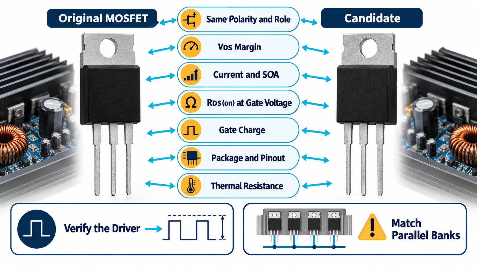
A MOSFET is an acceptable substitute in a car audio amplifier only when it matches the original device’s circuit role, polarity, voltage margin, current and safe operating area, on-resistance, gate charge, capacitance, package, pinout, and thermal behavior. There is no single list of “stronger” MOSFETs that safely replaces every amplifier transistor.
First determine whether the failed part belongs to the 12 V DC-DC power supply, a Class D output stage, a linear Class AB output stage, a protection switch, or another circuit. Parts that look identical can be optimized for completely different jobs. The overview of what MOSFET means in car audio explains these roles.
Identify the MOSFET’s job before choosing a substitute
Power-supply MOSFETs switch battery current through a transformer primary at tens or hundreds of kilohertz. They normally need low RDS(on) at the driver’s real gate voltage, high pulsed-current capability, good avalanche or unclamped-inductive behavior where specified, and manageable gate charge. Their voltage rating must tolerate the battery, transformer leakage spikes, load dump protection strategy, and ringing.
Class D output MOSFETs switch the audio waveform into an output filter and speaker. Their reverse-recovery behavior, output capacitance, gate charge, switching loss, dead-time behavior, and linearity all influence efficiency, distortion, and shoot-through risk. A lower RDS(on) part with much larger charge can run hotter because the existing driver switches it too slowly.
Class AB amplifiers may use lateral MOSFETs or bipolar transistors in a linear output stage. A switching MOSFET is not automatically a valid substitute. Transconductance, threshold distribution, capacitance, thermal coefficient, bias network, safe operating area, complementary pairing, and mounting arrangement become central.
Parameter 1: channel type and topology
Replace N-channel with N-channel and P-channel with P-channel unless you are redesigning the circuit. Confirm whether the device is used high side, low side, in a push-pull primary, synchronous rectifier, half bridge, or linear complementary pair. The MOSFET symbol, transformer connection, and driver outputs help identify the role.
Some packages contain two MOSFETs or an integrated driver and FET. Others include a Kelvin source or special pin arrangement. A visually similar three-lead package does not guarantee the same internal function.
Parameter 2: voltage rating and transient margin
The substitute’s VDS rating must be at least as high as the original and should preserve the designer’s transient margin. A car electrical system can experience jump-start, alternator, switching, and load-dump disturbances, although the amplifier’s front-end protection may clamp part of them. Transformer primary ringing can raise drain voltage far above the nominal battery value.
Do not choose an extremely high voltage rating without checking resistance and charge. Higher-voltage die may have more RDS(on) or capacitance in the same package. The best replacement has enough margin, not the largest possible number.
Parameter 3: current, pulsed current, and SOA
Datasheet current ratings are often limited by an ideal case temperature or package connection that the amplifier does not achieve. Compare continuous current under realistic thermal conditions, pulsed current for the switching cycle, and the safe operating area for the pulse duration. Linear output devices require especially careful SOA comparison because they can carry high current and voltage simultaneously.
A claimed 200 A rating does not mean the leads, PCB, and heatsink can carry 200 A continuously. Use loss and temperature calculations such as those in the MOSFET heat-sink sizing guide.
Parameter 4: RDS(on) at the actual gate voltage
Compare on-resistance at the gate voltage delivered by the amplifier, not only at the datasheet’s best test condition. A logic-level part may specify resistance at 4.5 V, while another requires 10 V. In some car-audio supplies the driver produces 10 to 12 V; in compact Class D stages it may be lower.
Use the hot RDS(on), which can be significantly higher than the 25 °C value. Estimate conduction loss from RMS current and duty cycle. A lower cold resistance can be offset by poor thermal contact or a larger temperature coefficient.
Parameter 5: gate charge and capacitance
Total gate charge, Miller charge, input capacitance, reverse-transfer capacitance, and output capacitance determine how the existing driver interacts with the MOSFET. If the replacement requires much more gate charge, transitions slow down, switching loss increases, and the driver may overheat. If it switches much faster, voltage overshoot, EMI, and cross-conduction can increase.
Compare gate-charge curves at a similar drain voltage and current, not just one capacitance value measured at a different condition. Confirm that the driver supply and gate resistors keep VGS inside the substitute’s limits. More detail is available in gate-resistor tuning for efficiency and EMI.
Parameter 6: body diode and reverse recovery
In a half bridge or Class D output, the body diode may conduct during dead time. Reverse-recovery charge and peak recovery current can affect switching loss, ringing, and shoot-through. Some low-voltage MOSFETs optimize third-quadrant behavior, while linear devices may not be characterized for fast commutation.
Do not add or remove an external diode unless the topology and timing are understood. The Schottky diode guide explains where a separate fast diode may help, but it is not a universal repair.
Parameter 7: package, pinout, and mounting
Confirm gate, drain, source, tab, exposed pad, and Kelvin-source connections against both datasheets. Check lead pitch, body height, insulation pad, screw location, creepage, copper footprint, and heatsink pressure. Reversing drain and source can leave the body diode permanently in the wrong current path even if the part appears to switch on.
Thermal resistance must be compared through the actual interface. Replace cracked mica, silicone pads, shoulder washers, or dried thermal compound. Verify electrical isolation between tab and heatsink where the design requires it.
Should all parallel MOSFETs be replaced?
If one device in a paralleled bank failed catastrophically, its neighbors may have absorbed excess current or gate stress. Many repair procedures replace the full bank with parts from the same manufacturer and lot, especially when static and dynamic sharing matter. At minimum, compare gate threshold, RDS(on), leakage, and switching behavior, and follow the service manual.
Mixing old and new parts with different gate charge can make one device turn on first or turn off last. Unequal source resistance, thermal contact, or gate routing can further unbalance current. Matching does not cure damaged drivers or poor bus layout.
Checks before powering the repaired amplifier
- Test the gate-driver outputs without the power MOSFETs when the circuit permits.
- Check gate resistors, driver transistors, bootstrap parts, dead-time components, and gate clamps.
- Test transformer windings, rectifiers, output devices, and the speaker load for shorts.
- Inspect snubbers, current-sense resistors, bus capacitors, and solder joints.
- Mount the replacement bank with correct isolation and torque.
- Power from a current-limited bench supply at reduced voltage if the service procedure allows.
- Observe gate waveforms and drain overshoot with appropriate isolated probes before applying full load.
- Run a thermal soak and distortion or output-power test.
A shorted MOSFET is often a symptom rather than the root cause. Review MOSFET heating mechanisms before treating a cooler-running replacement as proof that the repair is complete.
Frequently asked questions
Can I substitute a MOSFET with a higher current rating?
Only if the other requirements also match. Higher current may come with greater gate charge, different SOA, pinout, capacitance, or package thermal behavior.
Is lower RDS(on) always better?
No. It lowers conduction loss, but a larger die may increase gate charge and switching loss. Compare total loss with the existing driver and frequency.
Can I replace only the visibly burned MOSFET?
Sometimes, but parallel or complementary banks often require matched replacement. Test neighboring devices and follow the amplifier’s service guidance.