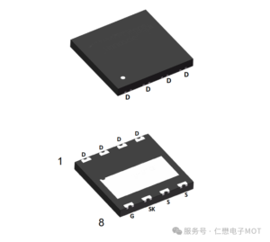
Scene: Your power drive and battery protection panels burn MOSFET, or battery protection systems fail after a sudden wave. The source of the problem is often not normal working currents, but the instant peaks of the voltage that the oscillators can't capture — avalanches of energy are sneaking around.
Hello, I'm an application engineer in power electronics. Today, without talking about empty theories, we go straight into a key parameter that is easily ignored in the selection, but is sufficient to determine the success or failure of the project: single-pulse avalanche energy. I'd like to share with you, for example, why I value its EAS capabilities so much.
EAS tests are usually based on sensory load switches.
The underlying principle is to control the MOSFET conductivity through a gridding signal, which is charged to a cascade; and when the MOSFET is cut off, the energy stored in the sensor is released through the device, forcing the leaking voltage VDS to rise and may exceed its blasting voltage BV DSS into avalanche. Test until the device fails and calculates the energy consumed on the basis of parameters such as currents before the failure.
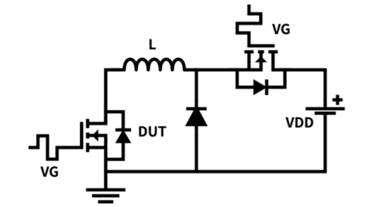
A typical test method is to set the main-line voltage V DD, to apply a pulsed voltage (e. g. , 10V) to conduct the device between the source poles of the fence, and to increase the electrons current to a specific value of I AS after-off. EAS is measured or calculated by electro-sensor energy releases resulting in avalanches. It should be noted that accurate EAS calculations should use BV DSS values measured in actual tests rather than directly using manual labels, and that testing conditions may vary from plant to plant, so that the EAS capabilities of different devices cannot be directly compared with specifications values alone.
EAS: Not "paper parameters", but "safe wire" for circuits
In assessing a MOSFET, we first look at the basic parameters of Vds, Rds (on), Id. But unlike EAS, it measures the survival of the device in extreme accidents. Imagine that when the power is shut down, relays are cut off or the circuits are hit by thunderstorms, huge sensory energy is turned into high-pressure peaks, which are applied directly to the missing source pole of MOSFET. At this point, if the EAS capability of the device is insufficient, the result is only one: an instant bomb.
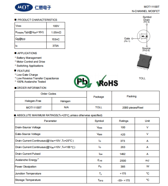
In the data manual, Jin Zhen MOT1115BT clearly marked its EAS value as 2500 mJ (at TJ = 25°C, L = 0. 5 mH). What does that mean? It amounts to a powerful energy absorber for your circuits, capable of eating destructive energy up to 2. 5 joules at a critical time and providing valuable buffer space for the system.
Three, MOT, high-level EAS behind Mot1115BT, is solid engineering reliability.
The EAS capability of a MOSFET is not based on empty space, but is derived from the hard power of the chip design and containment process.
“100% Avalanche Tested” commitment: this is one of the most reassuring points of MOT1115BT. This means that each of the out-of-plant devices has been screened through avalanche energy tests. This avoids individual differences due to process fluctuations and ensures the consistency and high reliability of bulk products, which are essential to our pursuit of projects that stabilize production.
2. Excellence in thermal performance is fundamental: the essence of the EAS event is energy to heat. MOT1115BT is extremely low as thermal resistance to the shell is only 0. 39°C/W. This means that the huge heat generated during the avalanche process can be rapidly exported from the core of the chip while keeping the temperature of the hot spot low, thereby significantly increasing its energy tolerance limits. Combined with TOLL-packaged large-sized dissipated welders, the dissipation efficiency is much greater than the traditional equivalent.
3. Robust body diodes: EAS failure is mostly related to aerobic avalanche penetration of the parasite. The MOT1115BT bipolar tube is capable of pulsating currents of 1492A, which provides a double guarantee of stability in its continuation and avalanche conditions.
IV. Operational choice: How can you simplify your design using the EAS advantage of MOT 1115BT?
Understanding the robustness of MoT1115BT, we can do more to design the system:
Reduced dependence on absorbent circuits: Although we still recommend the use of absorbent circuits such as RDCs or TVS, the high EAS value of MOT1115BT can reduce the stringent requirements for absorbent component performance. In space or cost-limited design, a MOSFET that is itself more “anti-beating” can significantly enhance the system's robustness.
• Responding to unpredictable surges: some of the peaks in voltage originate from the complex electromagnetic environment in the field and are difficult to completely simulate in laboratories. The selection of EAS-capable devices amounts to an insurance policy for these “unknown risks”.
• Extending the life of the system: even within the size of the design, frequent small-energy avalanches can gradually damage the device. The high tolerance of MOT1115BT can effectively slow down this ageing, especially in the fields of industry, automobile electronics, which require long-term reliable operation.
Engineer's choice.
In many years of project experience, I have learned that the quality of products often depends on the intensity of the weakest links in the worst of conditions. Not only does Jin Zhen Mot1115BT provide 1. 05 m low-conducted electrical resistance and 373A large current capacity, but its 2, 500 mJ EAS value is a serious commitment to reliability. It gives me greater confidence in responding to sudden-onset situations when designing power drives, large current power, battery management systems.
The choice is to fill your product with a strong "pressure-resistant heart" that can meet the power challenges of the real world.