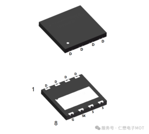
In the hardware design of wirelessly charged products, the selection of power switches directly determines the energy conversion efficiency, power density, heat performance and long-term reliability of the product. The MOT3145J N Tunway MOSFET, which is electronically launched, with ultra-low-conductive electrical resistance, high current carrying capacity, fast switch characteristics and compact PDFN3X3 containment, perfects the power switches, synchronized currents and load switching needs of the wireless charge emitter/receiving end, especially for the 15W-50W large power-free fast charge program, and is the preferred option to accommodate performance and small-scale design.
Core performance requirements for wireless charge-to-power MOSFET
Wireless charge is based on the principle of electromagnetic induction for energy transmission, the entire bridge/half-bridge reverse circuit at the launch end, the synchronous whole-flow circuit at the receiving end is dependent on MOSFET ' s high-frequency switch action, while the lightweight, fast-filling trend of the equipment imposes stringent requirements on the device:
1. Low-conductive electrical resistance: reduce lead-through losses in large currents, increase energy conversion efficiency and reduce temperature rise;
High current capacity: to meet the demand for large and sustained currents and pulsed currents in a fast-charging scenario and to cope with load fluctuations;
3. Rapid switch properties: the working frequency of the fit-for-wire charge of dozens of kHz, reducing switch losses and controlling EMI;
4. Small encapsulation + Good Heat Performance: small layouts suitable for wirelessly charged products to ensure heat dispersion reliability under high power;
5. Low-barrel polar charge: reduce driving wear and tear, simplify driving circuit design, adapt to low-cost MMU/drive chip drive.
The electrical properties of MOT3145J, on the other hand, are highly compatible with the above-mentioned needs and constitute an ideal option for wireless charge design.
II. MOT3145J Core Performance Advantages for Appropriate Wireless Charges
Combining the parameters of the specifications of the device, from the actual application scene of wireless charge, the core advantages can be summarized in five dimensions, fully covering the performance requirements of the core application scenario such as power switches, synchronized currents, load switching, etc. :
1. Ultra-low-conductive electrical resistance, resulting in extremely low-conductive wear and tear
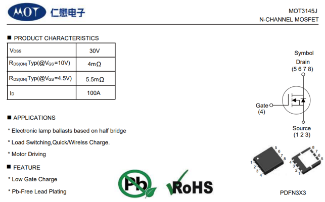
MOT3145J when VGS = 10V, ID = 20A, the typical RDS (ON) value is only 4 m, with a maximum of 5 m; even if the low pressure drive (VGS = 4. 5 V, ID = 20A), the typical RDS (ON) value is only 5. 5 m, much better than the standard MOSFET.
In the entire bridge circuit at the wireless charge launcher end, leading losses are the main source of power losses, calculated by formula **P cond=I rms2xRDS (ON)**, using 15W as an example, the flow of rms in the launch end reverse transformer circuits is about 8A, MOT3145J single pipe conduit losses are only 0. 256W, and total loss of four tubes is less than 1. 1W, which is 60 per cent lower than that of RDS (ON)=10m, significantly increasing the efficiency of the machine while reducing heat.
2. High current carrying capacity, adequate for high current demand
The device continues to leak the extreme current ID up to 100A under 25 °C and remains at 79A at high temperatures, and the pulse current IDM is up to 400A, fully covering the 15W-50W wireless current demand.
In the wireless charge process, there is a load mutation, an object detection transient current pulse, the high-pulse current capacity of MOT3145J can respond effectively to such peak currents and avoid overflow damage to the device; at the same time, the high and sustained current capacity also provides a residual amount for product power upgrades, so that a single device can meet the need for wireless currents within 30W without multiple tubes and connections to simplify circuit design.
3. Quick Switch + Low-barrel charge, balancing efficiency with EMI control
MOT3145J has excellent dynamic switch characteristics: td (ON) = 6ns, uptime td (OF) = 32ns, downtime tf = 8ns, the switch is fully equipped with a wireless charge of 40 kHz-150 kHz.
At the same time, its general grid charge Qg is only 31. 3 nC, its supply charge Qgs = 3. 7 nC, and the low grid charge means that the chargeable loss of the driveway is lower and can be directly reduced by a low-cost grid-driven polar chip or MPU GPIO (with simple driver resistance); and it is flexible to adjust the switch edges (e. g. 6-25 times) to balance the switch loss with EMI and avoid the electromagnetic radiation from high-frequency switches.
4. PDFN3X3 Small Envelope + High Heat Performance, Fit to Smaller Layout
MOT3145J uses PDFN3X3 seals, 3mmx3mm of plate area, with significant savings in PCB space, perfectly adapted to the layout requirements of light-lined products such as wireless charging floors, magnetic insorption wireless charge, etc. , and provides for more sheet space for other devices, such as wires, resonating the electrical caps, and master control chips.
The encapsulated crusts heat retardation RthJC is only 1. 56 °C/W, combined with a naked welding plate at the bottom of the encapsulation, designed by PCB for a large area of copper (2oz copper thick) and dispersed perforation, which quickly removes the heat during the work of the device, even under 50W power, the temperature of the device can be contained in a safe range (maximum TJ = 150 °C), avoiding heat-reducing power and ensuring continuous speed stability.
5. 30V + perfect reverse properties to meet circuit voltage stress requirements
Direct current parent voltage at the end of the wireless charge launcher is usually 12V/20V, with leaks from the receiving end in the form of approximately 5V-9V, and MOT3145J punching through the voltage VDSS=30V, leaving sufficient pressure tolerance for the peak of the voltage (real stress is below 70% of the rated value) to effectively absorb the voltage impulse during the switch and improve the reliability of the circuit.
At the same time, continuous current IS = 100A, pulsed current ISM = 400A, reverse recovery time tr = 45ns, reverse recovery charge Qrr = 22nC, and excellent bipolar properties that allow it to effectively reduce reverse recovery losses and further improve current efficiency at the receiving end in synchronous current applications.
III. Model application scenario for MOT3145J in wireless charge
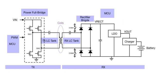
MOT3145J can be fully applied to the wireless charge end of the transmitter and the receiving end of the core circuit, covering the entire scene design from low to medium power. In the trend towards high power, fast recharge and miniaturization of wireless charge, the performance of MoSFET becomes a core bottleneck in product design. MOT3145J N Trench MOSFET, with ultra-low-conductive electrical resistance, high current capacity, fast switch properties, compact seals and excellent heat properties, perfectly adapted to the various applications of the wireless charge transmitter/receiving end, has fundamentally addressed the design pain points of efficiency, temperature rise and layout space.
As an application engineer, in practical design, the performance advantages of MOT3145J can be fully realized through rationally driven circuit design, PCB layout optimization, dissipation design and EMI control, leading to efficient, reliable and miniaturized wirelessly charged product design. The device not only applies to consumer products such as cellular wireless charger, wireless charger base, but also extends to industrial scenarios such as vehicle-borne wireless charger, smart home device wireless charger, and has a wide range of applications prospects.