


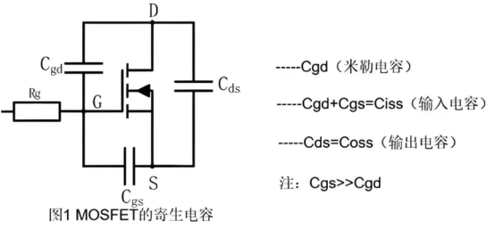
The Miller effect is a key issue that cannot be ignored in the design of large power MOS pipelines. This phenomenon is essentially caused by the physical properties of the leaking cap (Cgd) inherent in the MOSFETs, and any MOSFETs with Cgd would exhibit a different degree of miller effect.
Many start-up engineers lack in-depth knowledge of the Miller effect, especially in the area of small signal processing or low-power applications, and often consider the conductor of the MOSFETs as simple as the normal IO signal reversal. However, the reality is much more complex.
Let's take a look at the real wave-shaped signal on Vgs when the MOS pipe is open:
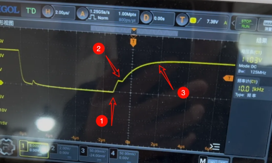
Three distinct stages can be clearly seen when observing the actual wave shape of Vgs during the opening of the MOSFETs. For small signals or low power MOSFETs, it is difficult to observe this phenomenon mainly because of insufficient time axis resolution. The presence of the Miller platform can be clearly seen with proper expansion of the wave-shaped time axis.
Now, let's analyze how the Miller platform was formed.
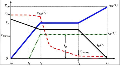
At t2, the smallest value of the reduction in Rdson's currents is set at Id, so the leaking currents reach their maximum, and Vds' voltage will fall fast, with different drop curves depending on the load, and will also be affected by the grid's polar currents, which will eventually be close to 0, i. e. , the MOSFETs will be fully steered.
The question is, why does Vgs not go up from t2? See:
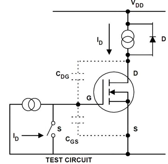
Why isn't Vgs voltage rising from t2? This is due to the presence of parasitic Cgd between the fences of the MOSFETs and the leakage poles. At t2, Vgd voltage will drop to near-0V depending on the load, and Cgd will need to be recharged as the voltage drops. If the charge speed matches Vgd's rate of decline, it creates a platform state where the voltage remains constant.
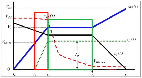
The loss formula for the MOSFETs is P=UxI, i. e. VdsxId. Throughout the process, t1-t2 and t2-t4 phases produce significant heat losses. At t1-t2, Vds had not yet completely declined, while Id ' s current had risen straight and Rdson had gradually decreased; at t2-t3, Id had reached its maximum, but Vds had not yet been minimized, which was the continuing process of the Miller platform.
Assuming that we now have a MOSFETs parameter of 100 V, 2 mR, its specifications provide the following dynamic parameters, let's analyze how to drive this MOS.
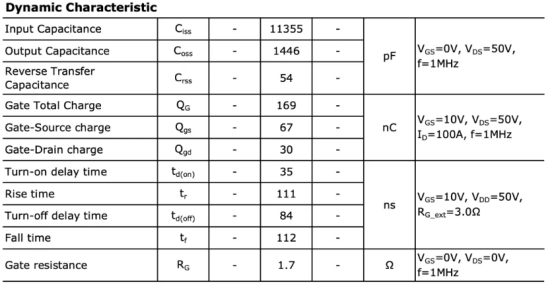
in the icon.
In practical applications, if the MOSFETs has been selected, switch losses can be reduced by boosting the power flow. An example is the MOS management of a typical parameter (100 V, 2 mR internal blockage), Qg named 169nC. If 2A-driven currents are provided, the theoretical opening time is only 84. 5 ns. However, in practical applications, factors such as grid-driven limit-to-flow resistance and changes in both ends of Miller ' s capacitation are also to be considered, usually for longer periods of time.
In the context of client technical support, the MOT FAE team found that rational selection of driving circuit parameters, combined with our optimized MOS products, could significantly improve the overall efficiency of the system. The technical programmes that we offer not only take into account the performance of the device itself, but also provide a complete solution for the client, fully integrated with the actual application scene.