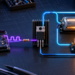
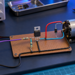
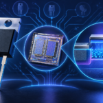
How do MOSFETs work? A MOSFET controls a conductive channel with the electric field produced by voltage on an insulated gate. Changing gate-to-source voltage changes the number of charge carriers in the channel, which changes the current that can flow between drain and source. The gate’s insulation explains both the high input resistance and the need to charge capacitance whenever the device switches.
This article follows an enhancement-mode N-channel MOSFET because it is the most common power-switching device. P-channel operation uses the opposite voltage polarity, while the same field-effect principle still applies.
Inside an N-channel MOSFET
A simplified MOSFET contains source and drain regions, a semiconductor body, a thin gate dielectric, and a gate electrode. At zero gate bias, the device structure prevents a low-resistance electron path between source and drain. Applying a positive voltage from gate to source attracts electrons toward the surface below the gate.
Once the electric field is strong enough, those electrons form an inversion layer: the channel. The channel connects the source-side and drain-side regions electrically. More gate overdrive generally increases channel charge and lowers channel resistance.
The gate dielectric prevents normal DC current from flowing into the gate. However, the gate, channel, drain, and source form capacitances. Every turn-on and turn-off event moves charge into or out of those capacitances.
Step-by-step turn-on process
- The driver raises the gate voltage. Current flows into the effective input capacitance and VGS rises.
- VGS reaches threshold. A channel begins to form and drain current starts increasing. Threshold is specified at a small test current, so the device is not yet fully on.
- Drain current reaches the load current. The circuit’s inductance or other load now determines current while drain voltage begins to change.
- The Miller plateau occurs. Gate current mainly charges the gate-to-drain capacitance while VDS falls. VGS changes slowly during this interval.
- The channel becomes fully enhanced. After VDS falls, VGS rises toward the driver voltage and the MOSFET reaches its low-resistance on state.
Turn-off reverses the sequence. The driver removes gate charge, VDS rises through the Miller interval, drain current transfers to another switch or diode, and the channel disappears as VGS falls.
Why the source voltage matters
A MOSFET responds to VGS, not gate voltage measured only against circuit ground. In a low-side N-channel switch, the source is close to ground, so a ground-referenced driver is straightforward. In a high-side N-channel switch, the source rises toward the positive bus when the device turns on. The driver must raise the gate above that moving source by the required amount.
Bootstrap drivers, isolated drivers, or charge pumps create this floating high-side drive. If the driver cannot maintain enough VGS, the MOSFET remains partially enhanced and may overheat.
The three main operating regions
Cutoff
Below the required gate voltage, the channel is absent or too weak to carry meaningful load current. The MOSFET behaves as an open switch, although leakage and capacitance remain.
Ohmic or linear region
With sufficient gate drive and relatively low VDS, the channel behaves approximately as a resistance. This is the desired on state for most switching applications. The instantaneous conduction loss is approximately I2RDS(on).
Saturation region
At higher VDS, the channel pinches near the drain and current depends mainly on gate overdrive. Analog amplifiers and current sources use this region. MOSFET saturation should not be confused with BJT saturation: a hard-on power MOSFET normally operates in the ohmic region.
What controls the drain current?
Drain current is not set by gate voltage alone. It is the result of the MOSFET characteristic and the external circuit. Important influences include:
- Gate-to-source voltage and available gate overdrive
- Drain-to-source voltage and operating region
- Load resistance, inductance, supply voltage, and other switches
- Junction temperature, which changes resistance and threshold behavior
- Source inductance and voltage drop shared with the gate-drive loop
- Device construction, die size, cell geometry, and process technology
For switching design, use datasheet curves only as a starting point. Curves often show typical values, while guaranteed limits appear in specification tables under defined conditions.
Gate charge matters more than gate DC current
Because the gate is capacitive, steady-state gate current is tiny, but switching gate current can be substantial. A rough average gate-drive current is Qg multiplied by switching frequency. Peak current determines how quickly the device crosses its high-loss transition interval.
For example, a device with 50 nC total gate charge switching at 100 kHz requires an average charge-transfer current of 5 mA. That number sounds small, yet a fast 50 ns transition may require much higher peak current. The gate driver and loop impedance must support both the average and peak requirements.
The Miller plateau and drain-voltage transition
The gate-to-drain capacitance couples drain-voltage movement back to the gate. During the Miller plateau, the driver supplies gate current while VDS changes. Approximate transition time depends on gate-to-drain charge divided by available driver current in that interval.
A smaller gate resistor or stronger driver can shorten switching time and reduce voltage-current overlap. Excessively fast edges can increase ringing, EMI, false turn-on, diode recovery stress, and voltage overshoot. Gate resistance is therefore a tuning element, not simply a value to minimize.
Where MOSFET power loss comes from
| Loss mechanism | Main drivers | Design response |
|---|---|---|
| Conduction loss | RMS current, duty cycle, RDS(on), and junction temperature | Use hot resistance, reduce current path resistance, and improve cooling |
| Turn-on and turn-off overlap | Voltage, current, transition time, and frequency | Optimize gate drive and layout; measure switching energy |
| Output-capacitance loss | Eoss, bus voltage, topology, and frequency | Compare stored-energy curves and evaluate soft switching |
| Gate-drive loss | Qg, drive voltage, and frequency | Choose suitable charge and efficient driver supply |
| Body-diode and reverse-recovery loss | Dead time, current, di/dt, Qrr, and temperature | Optimize dead time and commutation; consider device technology |
| Leakage and off-state loss | Voltage, temperature, and blocking time | Check hot leakage and standby requirements |
How the body diode works
The body-to-source connection inside a discrete N-channel power MOSFET creates a diode from source to drain. In bridge and synchronous circuits, this diode may carry current during dead time before the channel turns on. Its forward drop and reverse-recovery behavior can affect loss and overshoot.
Turning the MOSFET channel on can conduct reverse current with a lower voltage drop than the diode. This is the basis of synchronous rectification. Timing still matters: overlapping the high-side and low-side switches creates shoot-through, while excessive dead time increases diode conduction.
Temperature changes MOSFET behavior
RDS(on) commonly rises substantially as junction temperature increases. The resulting conduction loss raises temperature further, so thermal calculations should iterate with the hot resistance. Threshold voltage generally falls with temperature, while leakage rises. Switching and diode behavior can also change.
Junction temperature is estimated from power loss and the relevant transient or steady-state thermal impedance. The correct thermal path depends on pulse duration, package, PCB copper, interface material, heatsink, airflow, and ambient conditions.
Layout is part of MOSFET operation
Parasitic inductance converts fast current change into voltage. Drain-loop inductance produces overshoot and ringing. Common-source inductance subtracts from effective gate drive during turn-on and turn-off. Gate-loop inductance can produce oscillation. A compact power loop, separate gate-return path, local driver decoupling, and Kelvin-source connection where available make the measured circuit behave more like the datasheet test circuit.
A practical switching checklist
- Confirm VDSS margin against measured maximum drain voltage.
- Confirm the driver supplies the specified VGS at the MOSFET pins.
- Estimate hot RDS(on) conduction loss using RMS current.
- Estimate transition, Eoss, diode, and gate-drive losses at maximum frequency.
- Check safe operating area for startup, faults, and linear intervals.
- Measure VGS, VDS, current, ringing, and temperature with low-inductance probing.
- Repeat testing at supply, load, temperature, and component-tolerance corners.
Frequently asked questions
Why can a MOSFET stay on after the signal is removed?
The gate stores charge. If the gate is left floating, leakage, coupling, or static charge can maintain a voltage. A gate-to-source pull-down or pull-up resistor defines the off state, while a driver actively removes charge.
Why does a MOSFET get hot when switching?
It dissipates conduction loss while on and switching loss while voltage and current overlap. Output-capacitance energy, diode recovery, gate-drive loss, insufficient VGS, high frequency, and poor layout can add significant heat.
Can a microcontroller drive any MOSFET directly?
No. The MOSFET must have guaranteed low RDS(on) at the microcontroller’s output voltage, and the pin must move the required gate charge at the desired speed. Many power stages need a dedicated driver for current, voltage translation, timing, and protection.
Summary
MOSFETs work by using an insulated gate’s electric field to create and control a channel. That simple principle becomes a dynamic charge-control problem during real switching. Reliable design requires the correct VGS, adequate driver current, controlled commutation, low-inductance layout, realistic loss calculations, and thermal validation.