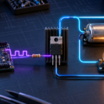
How do you wire a MOSFET? The answer depends on whether the device switches the low side or high side of the load. For the most common N-channel low-side circuit, connect source to ground, drain to the load, the other side of the load to the positive supply, and gate to the controller through a series resistor. Add a gate-to-source pull-down resistor and a flyback path for an inductive load.
Correct wiring must account for the actual package pinout, gate-to-source voltage, current return, body diode, voltage transients, and thermal path. A drawing copied from another MOSFET may be wrong if its leads use a different order.
Check the pinout first
Locate the exact datasheet and confirm gate, drain, source, and tab connections. Many TO-220 MOSFETs use gate-drain-source when viewed from the front, but exceptions exist. Surface-mount packages may expose several drain or source pins and a separate Kelvin-source pin.
The metal tab is often connected to drain. If several devices share a heatsink, use an insulating pad when required and account for its thermal resistance.
Basic N-channel low-side wiring
| Connection | Wire it to | Purpose |
|---|---|---|
| Source | Power ground or supply return | Provides the current return and gate-voltage reference |
| Drain | Low side of the load | Controls the load current path |
| Other load terminal | Positive load supply | Completes the power path when the MOSFET turns on |
| Gate | Controller or driver through a series resistor | Charges and discharges the gate capacitance |
| Gate-to-source resistor | Between gate and source | Defines the off state when the driver is high impedance |
The controller ground and MOSFET source must have a defined connection unless the gate driver is isolated. Without a common reference, a 5 V controller output does not guarantee 5 V VGS.
Where to place the gate resistor
Place the series gate resistor close to the MOSFET gate. It limits peak driver current and damps ringing created by gate capacitance and trace inductance. Typical starting values may range from a few ohms to several tens of ohms, but the correct value comes from waveform and EMI testing.
Use separate turn-on and turn-off resistors with a diode when the application needs different edge rates. A strong turn-off path can improve dV/dt immunity while a slower turn-on reduces ringing.
Where to place the pull-down resistor
Connect the N-channel gate-to-source pull-down physically close to the MOSFET. It must overcome leakage and capacitive coupling but not waste unnecessary controller current. Values such as 10 kΩ to 100 kΩ are common starting points, not universal rules.
For a P-channel high-side switch, use a gate-to-source pull-up instead. It keeps the gate at the source voltage and the device off.
Wire an inductive load
For a DC motor, relay, or solenoid controlled by a low-side N-channel MOSFET, connect a flyback diode across the load. Place its cathode at the positive supply and anode at the MOSFET drain. The diode is reverse biased while the MOSFET is on and conducts the inductive current after turn-off.
Keep the diode-current loop short. A remote diode connected through long wires may not control the local drain spike. If the load must release quickly, use a TVS, Zener clamp, active clamp, or higher-voltage recirculation strategy rather than a simple low-voltage diode.
Add local decoupling
Place a suitable capacitor close to the load-switching loop. The supply lead and wiring inductance can create voltage dips and spikes when current changes rapidly. Use a combination of bulk capacitance and low-inductance ceramic capacitance as appropriate for the current and frequency.
Connect the decoupling return directly into the power loop rather than forcing high switching current through the controller ground path.
Separate signal ground and power current
High load current through a shared ground trace creates voltage drop. If the driver references a distant ground, this drop changes the effective VGS. Route the driver return to the MOSFET source with a short, low-inductance path.
In high-current designs, use a Kelvin-source or dedicated source-sense connection for the gate driver. Keep current-sense and controller signals away from the switching loop.
Wire a P-channel high-side switch
Connect the P-channel source to the positive supply and drain to the load. Connect the other side of the load to ground. A gate-to-source pull-up holds the device off. Pull the gate lower to turn it on.
If a low-voltage controller cannot tolerate the supply voltage, use a small NPN transistor or N-channel MOSFET to pull the power MOSFET gate down. Add a resistor to limit pull-down current and a gate-source clamp when the supply could exceed VGS(max).
Wire an N-channel high-side switch
An N-channel high-side MOSFET normally provides lower resistance than a comparable P-channel device, but its gate must rise above its source. Use a high-side driver with a bootstrap capacitor, charge pump, isolated supply, or transformer-coupled drive.
A bootstrap driver needs switching activity to refresh its capacitor and may not support indefinite 100% duty cycle. Check startup behavior, minimum off time, driver undervoltage lockout, and source-node negative transients.
Wire two MOSFETs back-to-back
One off MOSFET still conducts through its body diode in one direction. To block current both ways, wire two MOSFETs so their body diodes oppose each other. Common arrangements connect source-to-source or drain-to-drain.
Battery protectors, electronic fuses, USB power paths, and reverse-current blockers use this topology. The driver must control both gates relative to the relevant source nodes.
Wire a half-bridge
A half-bridge uses one high-side and one low-side MOSFET around a switching node. Add a gate driver that controls both devices and inserts enough dead time to prevent shoot-through. Place the DC-link decoupling capacitor close to the bridge.
Keep the high-current loop formed by the capacitor and MOSFETs extremely compact. Minimize common-source inductance, separate driver return from power current, and manage switching-node copper to balance heat spreading against EMI.
Logic-level wiring example
Assume a 3.3 V microcontroller controls a 12 V, 2 A fan using PWM. A practical low-side arrangement includes:
- An N-channel logic-level MOSFET with RDS(on) specified at 2.5 V or 3.0 V gate drive.
- Source connected to the power return near the supply and fan return path.
- Drain connected to the fan negative terminal.
- Fan positive terminal connected to 12 V.
- Microcontroller output connected to gate through a small series resistor.
- A gate-to-source pull-down resistor.
- A flyback or transient-suppression path appropriate for the fan electronics and wiring.
- Local supply decoupling and a shared ground reference.
The MOSFET voltage rating must cover the 12 V supply and measured transients. The exact gate resistor, protection network, and PWM frequency require prototype testing.
Check wire and PCB current capacity
Use conductors, connectors, traces, planes, and vias that support the RMS current and acceptable voltage drop. A low-resistance MOSFET cannot compensate for a narrow trace or undersized connector.
Provide copper area or a heatsink for the expected loss. Thermal vias can connect a surface-mount package pad to internal or back-side copper. Follow the package land-pattern and assembly guidance.
Verify the wiring before power
- Confirm the device orientation and pin numbers against the datasheet.
- Check continuity from source to the intended return and from drain to the load.
- Confirm gate is not shorted to drain or source.
- Verify the pull resistor creates the safe default state.
- Check the flyback diode direction.
- Confirm the controller and gate driver stay within voltage ratings.
- Inspect for solder bridges and unconnected return paths.
- Use a current-limited supply for initial testing where practical.
Common wiring mistakes
- Swapping drain and source because the body diode makes the circuit partly work
- Connecting gate directly with no defined pull-down or pull-up
- Using gate-to-ground voltage instead of gate-to-source voltage
- Omitting a common reference between controller and source
- Reversing the flyback diode
- Placing the clamp or decoupling too far from the switching loop
- Routing driver return through the load-current path
- Driving a high-side N-channel gate only to the supply voltage
Frequently asked questions
Can I swap drain and source?
The enhanced channel can carry current in either direction, but the body diode, capacitances, internal body connection, and ratings make a discrete power MOSFET directional. Follow the intended orientation.
Does the gate need a resistor?
A pull resistor is strongly recommended to define the off state. A series gate resistor is often needed to control current, ringing, switching loss, and EMI. Its value depends on the driver and layout.
Where should the flyback diode connect?
For a low-side switch driving a DC inductive load, connect the diode across the load with cathode to positive supply and anode to the MOSFET drain.
Summary
Correct MOSFET wiring starts with the datasheet pinout. In a low-side N-channel circuit, source goes to return, drain goes to the load, and gate receives a controlled signal relative to source. Add a pull resistor, manage gate current, provide an inductive-current path, place decoupling close to the switching loop, and keep driver return separate from high load current. High-side and bidirectional circuits require additional driver and body-diode planning.