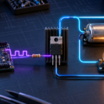
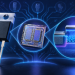
How does a MOSFET work in power electronics? A gate driver repeatedly charges and discharges the insulated gate. The resulting electric field turns a low-resistance channel on or removes it so the device can block voltage. Inductors, capacitors, diodes, transformers, and control timing then convert that rapid switching into a controlled voltage, current, torque, or power level.
The MOSFET is not a complete converter by itself. It is the high-speed valve in an energy path. Efficiency and reliability depend on the driver, switching loop, commutation path, passive components, cooling system, protection, and control algorithm.
The four stages of a MOSFET switching cycle
1. Off-state voltage blocking
With VGS near zero in an enhancement-mode N-channel device, no strong channel connects drain and source. The MOSFET supports the applied drain voltage, subject to leakage, capacitance, and its VDSS rating. The output capacitance stores energy while the device is off.
2. Gate charging and channel formation
The driver sources current into the gate. VGS rises through the threshold region and drain current begins to transfer into the MOSFET. During the Miller plateau, much of the driver current changes drain voltage through the gate-drain capacitance rather than increasing VGS.
3. Fully enhanced conduction
After the transition, the driver holds the intended gate voltage. The channel behaves approximately like RDS(on), and conduction loss is related to the square of RMS current. The actual resistance is higher at elevated junction temperature than the room-temperature headline value.
4. Turn-off and commutation
The driver removes gate charge. As the channel weakens, current transfers to a diode, another MOSFET, a clamp, or an alternative energy path. Parasitic inductance can create drain-voltage overshoot, while rapid dV/dt can couple through the Miller capacitance and disturb the gate.
A low-side switch example
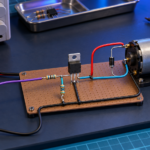
In a low-side N-channel circuit, the load connects to the positive supply and the MOSFET sits between the load and ground. A high gate voltage relative to the source turns the device on, completing the current path. Pulling the gate to the source turns it off.
For a resistive load, current falls rapidly at turn-off. For an inductive load, current cannot stop instantly, so a flyback diode, active clamp, synchronous switch, or other recirculation path is essential. Without it, the drain voltage rises until parasitic capacitance, avalanche, or breakdown absorbs the energy.
How a half-bridge uses two MOSFETs
A half-bridge places one MOSFET above the switching node and another below it. The controller alternates them to connect the node to the positive bus or the return. This arrangement appears in buck converters, synchronous rectifiers, class-D amplifiers, motor drives, and inverter stages.
The two devices must not conduct strongly at the same time because that would create shoot-through across the supply. A short interval called dead time is inserted between transitions. Too little dead time risks cross-conduction; too much dead time forces current through a body diode or third-quadrant path and can raise loss.
Why the high-side gate needs special drive
An N-channel high-side MOSFET requires its gate to be driven above its source. Since the source moves with the switching node, a ground-referenced logic output cannot maintain the necessary VGS. Bootstrap drivers, charge pumps, isolated gate supplies, or transformer-coupled drivers solve this problem.
A P-channel MOSFET can simplify a modest-voltage high-side switch because its gate is pulled below its source to turn on. At higher current, N-channel devices are usually preferred because they often provide lower resistance and better switching performance.
Where MOSFET power loss comes from
| Loss mechanism | Useful first estimate | Main design levers |
|---|---|---|
| Channel conduction | IRMS2 × RDS(on) | Hot resistance, gate voltage, die size, duty cycle, cooling |
| Voltage-current overlap | Approximately 0.5 × V × I × (tr + tf) × fSW | Driver current, gate resistance, layout, device charge, topology |
| Gate drive | Qg × Vdrive × fSW | Gate charge, drive voltage, frequency |
| Output capacitance | Related to Eoss per transition | Device capacitance, bus voltage, soft switching, frequency |
| Body diode and recovery | Forward drop, conduction time, and recovery energy | Dead time, commutation rate, diode behavior, topology |
| Linear or avalanche stress | Waveform energy over the event | SOA, clamps, snubbers, control response, transient margin |
These equations are starting points. Real switching waveforms are nonlinear, capacitances vary with voltage, and common-source inductance changes effective gate drive. Prototype measurement is required for an accurate loss budget.
How MOSFETs behave in common converter topologies
| Topology | MOSFET role | Critical behavior |
|---|---|---|
| Buck converter | High-side switch chops the input; low-side device or diode carries freewheel current | Dead time, reverse recovery, switching-node ringing, high-side drive |
| Boost converter | Low-side MOSFET stores energy in the inductor, then releases it through the output path | Drain-voltage stress, diode commutation, current peak, turn-off overshoot |
| Flyback converter | Primary MOSFET magnetizes the transformer and then blocks reflected output voltage | Leakage-inductance spike, clamp loss, avalanche margin, current sensing |
| Synchronous rectifier | MOSFET channel replaces a diode during the correct current interval | Timing, reverse current, body-diode interval, low RDS(on) |
| Motor inverter | Three half-bridges synthesize phase voltages with PWM | Shoot-through prevention, dV/dt, current recirculation, thermal cycling |
| Load switch or e-fuse | MOSFET connects, disconnects, or limits a power rail | Inrush, linear SOA, reverse blocking, short-circuit response |
Gate voltage versus gate charge
The controller decides the desired voltage, but the driver must deliver charge quickly enough to reach it. A MOSFET with large total gate charge can switch slowly when driven from a weak microcontroller pin. Slow transitions increase the time when voltage and current overlap.
Increasing driver strength or reducing gate resistance can lower switching loss, but faster edges may increase ringing, electromagnetic interference, diode recovery stress, and false turn-on. Gate resistance is therefore a system tuning component, not simply an obstacle to remove.
The body diode and reverse conduction
The body diode provides a current path when the channel is off and current polarity demands conduction. In bridge circuits, it may conduct during dead time before the complementary MOSFET turns on. When the channel is enhanced, current can flow through it in either direction, often with lower voltage drop than through the diode.
Body-diode reverse recovery can add current spikes and loss as another switch commutates the current. Datasheet Qrr is useful, but its value depends on current, temperature, dI/dt, and test circuit. Designers should evaluate it under conditions close to the actual converter.
Choosing a MOSFET for power switching
- Set the voltage class. Include supply tolerance, reflected voltage, ringing, surge, and abnormal conditions. Validate with measurement.
- Use hot resistance. Estimate RDS(on) at the expected junction temperature and available gate voltage.
- Evaluate switching figures. Review Qg, Qgd, Coss, Eoss, reverse recovery, and application-specific switching energy.
- Check the package and thermal path. Include junction-to-case or junction-to-board resistance, PCB copper, interface material, heatsink, airflow, and ambient temperature.
- Verify SOA and transient ratings. Startup, current limiting, short circuits, unclamped inductive switching, and hot-plug events may operate outside normal switching conditions.
- Prototype the real loop. Measure gate voltage, drain overshoot, current, switching energy, temperature, and EMI at operating extremes.
Layout is part of how the MOSFET works
PCB inductance and resistance can change device behavior. The high-current switching loop should be short and compact. Driver-to-gate and driver-return paths should also be short, with the return referenced to the source in a way that minimizes common-source inductance.
Place local decoupling close to the bridge, use appropriate copper width and layer transitions, and keep sensitive control traces away from the switching node. Kelvin-source packages or separate source-sense connections can improve gate-drive accuracy in high-current designs.
How to measure switching correctly
- Measure VGS between gate and source at the device, not gate to a distant ground point.
- Use a probe and ground connection with sufficient bandwidth and very low loop inductance.
- Use a differential probe rated for the common-mode and drain voltage when required.
- Measure current with a suitable shunt, current probe, or calibrated current transformer.
- Integrate instantaneous VDS × ID over the transition when estimating switching energy.
- Test maximum input, load, switching frequency, ambient temperature, startup, shutdown, and fault states.
Common misconceptions
The lowest RDS(on) MOSFET is always best
A larger die can reduce resistance while increasing charge and capacitance. At high frequency, a device with slightly higher resistance may produce lower total loss.
Threshold voltage is the required drive voltage
Threshold is specified at a small current. It marks the start of channel formation, not full enhancement. Use guaranteed on-resistance data at the actual drive voltage.
An avalanche rating eliminates the need for a clamp
Avalanche capability is limited by energy, starting temperature, repetition, and current distribution. Repetitive avalanche can reduce reliability even when a single pulse appears to fit an absolute-maximum rating.
A MOSFET conducts only from drain to source
The enhanced channel can conduct either way. The package convention, body diode, capacitances, and datasheet ratings still give the device a defined orientation.
Frequently asked questions
Why does a MOSFET get hot while switching?
Heat can come from channel resistance, slow transitions, gate drive, output capacitance, body-diode conduction, reverse recovery, avalanche, or linear operation. Insufficient cooling and unexpected RMS current make the temperature worse.
Can a microcontroller drive a power MOSFET directly?
Sometimes, at low frequency with a logic-level device and modest gate charge. At higher current or frequency, a dedicated gate driver usually provides faster, controlled transitions and better protection.
What turns a MOSFET off?
The driver removes gate charge and brings VGS below the level that sustains the required drain current. A pull-down resistor provides a defined off state when the driver is high impedance.
Why are two MOSFETs used back-to-back?
A single off MOSFET still has a body-diode path in one direction. Two devices with opposing body diodes can block current in both directions for battery protection, power-path control, and electronic disconnects.
Summary
A MOSFET works by using an insulated gate to create or remove a conductive channel. In power electronics, the driver repeats that process at controlled times so inductors, capacitors, transformers, and loads receive the desired energy. Real performance is shaped by gate charge, Miller behavior, on-resistance, output capacitance, body-diode commutation, parasitic inductance, thermal impedance, and protection. The best design treats the MOSFET, driver, layout, and energy path as one switching system.