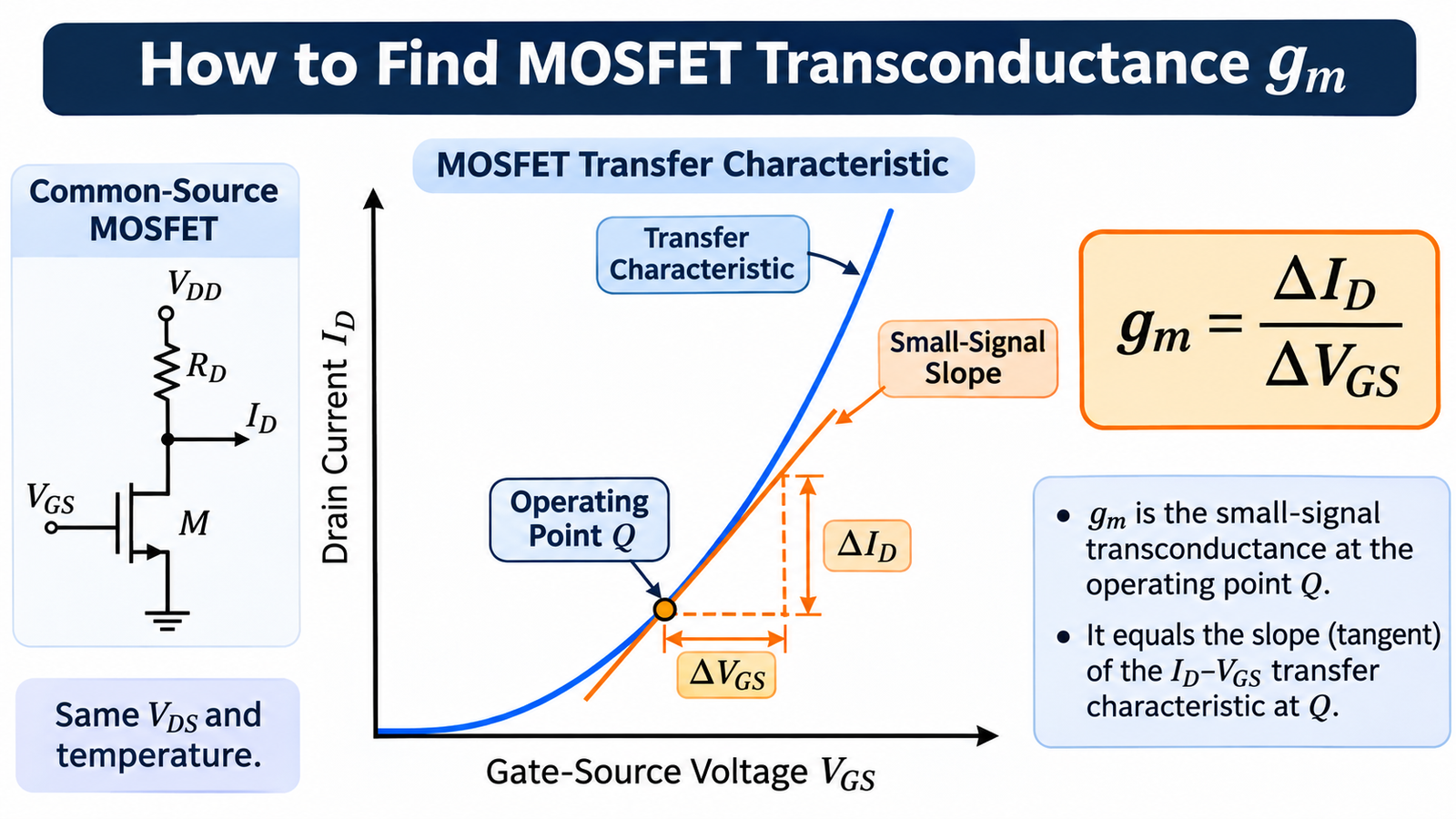
MOSFET transconductance, written gm or gfs, is the small-signal change in drain current divided by the change in gate-source voltage at a specific operating point: gm = ∂ID/∂VGS. Find it from the tangent slope of the ID–VGS transfer curve while holding VDS and temperature constant. It is not the same as threshold voltage, and it changes strongly with drain current and temperature.
What gm means in a MOSFET
The small-signal definition is:
gm = ∂ID / ∂VGS | VDS, TJ
The unit is siemens (S), equivalent to amperes per volt. A gm of 5 S means that a sufficiently small 10 mV change in VGS produces approximately a 50 mA drain-current change around that operating point, provided VDS, temperature and operating region remain effectively constant.
This local linearization is the controlled-current-source term in a MOSFET small-signal equivalent circuit. It helps predict voltage gain, loop gain and how strongly gate noise or ripple modulates drain current.
Read gm from a transfer curve
- Select the ID–VGS curve measured at the VDS and junction temperature closest to the intended operating point.
- Mark the required quiescent drain current and find the corresponding VGS.
- Choose two nearby points on either side of that operating point.
- Calculate
gm ≈ ΔID / ΔVGS. - Use progressively closer points if the graph resolution allows, or draw a tangent and calculate its slope.
For an illustrative graph, if current changes from 1.6 A to 2.4 A while VGS changes from 3.40 V to 3.50 V, the local estimate is 0.8 A / 0.10 V = 8 S. That value applies only near the midpoint and only under the graph’s stated VDS and temperature.
Do not confuse gm with threshold voltage
VGS(th) is measured at a small specified drain current and only indicates where conduction begins under the data-sheet test. It does not tell you the gate voltage required for low RDS(on) or the gm at load current. The transfer curve becomes steeper as current rises, so gm near threshold can be much lower than gm at a power operating point.
First confirm the device’s operating region with the method in checking MOSFET operating region. A gm extracted in saturation cannot be inserted blindly into a circuit operating deep in the linear or ohmic region.
Use equations only within their assumptions
For a long-channel enhancement MOSFET following a square-law model in saturation, an approximation is:
gm ≈ 2ID / VOV, where VOV = VGS − VTH.
The same model can be written gm ≈ √(2kID) when the process parameter k is known. Modern power MOSFETs do not follow this simple model over their complete current range. Cell structure, source resistance, mobility reduction, self-heating and package resistance all change the measured slope. Prefer data-sheet curves or measured data for power design.
Measure gm on the bench
Bias the MOSFET at the intended ID and VDS using a current-limited fixture. Apply a small gate-voltage perturbation and measure the corresponding drain-current change. Keep the perturbation small enough that the curve is locally linear, but large enough to exceed instrument noise. Pulsed measurements reduce self-heating; continuous measurements must track junction temperature.
- Use Kelvin source sensing when source-lead voltage drop would corrupt VGS.
- Record pulse width, duty cycle, VDS, ID and estimated TJ.
- Repeat at the temperature limits if gm affects stability or gain margin.
- Do not exceed the safe operating area while biasing the device linearly.
How gm affects circuit behavior
In a common-source stage, a simplified unloaded voltage gain is approximately Av ≈ −gm × Rload,effective. Real gain is lower because output resistance, source degeneration and external loading matter. In switching applications, higher gm can make current respond sharply to gate-voltage disturbances; that helps fast transition but also increases sensitivity to common-source inductance and false turn-on.
Use gm together with the current calculation in MOSFET drain-current analysis and the broader explanation of MOSFET current amplification.
Why data-sheet gfs may not match your result
A headline forward-transconductance value is commonly measured at one drain current, VDS and pulse condition. It may be typical rather than bounded by minimum and maximum limits. Your circuit can produce a different value because source and bond-wire resistance add degeneration, the junction is hotter, or VDS is too low to maintain the stated region.
Digitizing a printed graph also introduces slope error. Use several closely spaced points, fit a short local line and report the interval. If gm is important to loop stability or analog gain, measure more than one device lot and include the spread in the model.
gm extraction checklist
- The operating point, VDS and temperature are defined.
- The slope is local to the selected point.
- Typical data are not treated as guaranteed limits.
- Self-heating and source resistance are controlled.
- The extracted value is used in the correct operating region.
For device selection based on current, voltage, RDS(on), gate charge and thermal limits—not gm alone—review MOT’s power MOSFET portfolio.