Calculate VGS as gate voltage minus source voltage at the MOSFET pins. The source may move substantially in high-side, switching, or current-sense circuits, so gate voltage relative to ground is often insufficient.
VGS determines enhancement and gate-oxide stress. It must be evaluated dynamically, not only with a DC meter reading.
Start with the requirement
Define the source reference, drive voltage, source resistance or inductance, topology, and maximum positive and negative gate excursion.
Define the operating range before selecting a part, changing a connection, or doing a calculation. Record the normal value, the allowed tolerance, the maximum transient, the load waveform, the ambient condition, and the expected fault response. A nominal label or one typical data-sheet number is not a complete design requirement. For the underlying operating principles, review MOSFET operating basics.
Use the relevant electrical model
Use the driver schematic to calculate steady values, then include source bounce and Miller coupling during switching.
Use data-sheet curves at the appropriate current, voltage, temperature, and pulse condition. A maximum rating is a survival boundary, not a target operating point. Include wiring resistance, PCB parasitics, connector limits, measurement uncertainty, and control timing because any of them can change the measured result. The MOSFET wiring guide provides additional connection context when terminal orientation or current paths affect the calculation.
Check practical limits
Check the recommended drive range, absolute maximum VGS, UVLO behavior, gate-clamp voltage, and turn-off margin.
Review steady-state operation as well as startup, shutdown, load steps, and credible faults. In power circuits, an apparently small overshoot or short transition can dominate device stress. Measure at the component pins whenever possible, using a suitable probe and a short measurement reference. Use the MOSFET protection guide to place the result within the wider protection or design strategy.
Implement and validate
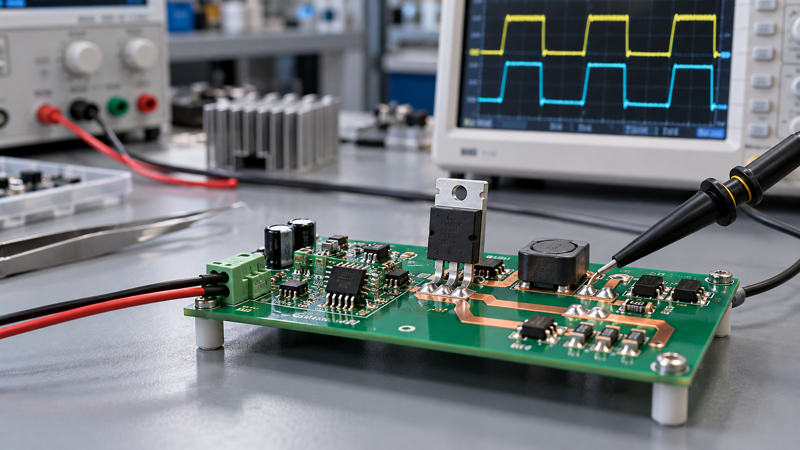
Probe gate-to-source directly with an appropriate differential or short-ground method.
Start with limited available energy where practical. Test the normal load, the expected worst load, temperature rise, and one relevant fault. Record the test arrangement and waveform. This makes later comparison meaningful and prevents a replacement part or wiring change from silently reducing margin.
Common mistakes
Do not compare gate voltage to ground when the source is not at ground.
Do not rely on a circuit that only works briefly at room temperature. Repeat the relevant test after warm-up and in the intended enclosure. A safe design should also reach a defined state when a control signal, sensor, connector, or auxiliary supply is absent.
Build margin into the complete assembly
A component calculation is only useful when it represents the complete assembly. The final behavior also depends on traces, connectors, source impedance, board layout, parasitic inductance, thermal interfaces, surrounding heat sources, firmware timing, and the measurement method. A circuit may pass a short bench check but still fail at a supply extreme, a hot enclosure temperature, a load transient, or a connector fault. Treat every calculated value as a starting hypothesis that needs a stated operating boundary.
Create a short requirement table before changing hardware. List the nominal and maximum input, output or device voltage, continuous and peak current, frequency or timing, load type, maximum ambient, thermal route, protection components, and the acceptance limit for the finished circuit. Use data-sheet values that match these conditions. When curves show typical performance, leave appropriate margin for production spread and temperature. This helps prevent a low room-temperature resistance, a typical threshold, or a nominal current rating from being mistaken for a guaranteed application limit.
Measurements should be planned with the same care. Measure at the actual device or load terminals, state the probe reference and bandwidth, and avoid introducing an antenna loop with a long ground lead. Keep a record of the part number, supply setting, load, ambient, circuit revision, and waveform or reading. If an unexpected result appears, preserve the setup and test one change at a time. These habits make it possible to distinguish a component limitation from a layout, connection, or instrument artifact.
Finally, decide how the circuit behaves when something goes wrong. A floating gate, disconnected sensor, supply brownout, reversed connection, or shorted load should lead to a deliberate condition. Use the relevant fuse, current limit, clamp, pull resistor, isolation barrier, or shutdown function for a defined purpose. A safe and documented failure response is part of a reliable electrical design, not an optional afterthought.
Engineering checklist
Document the part number, input and output range, current, temperature, protection parts, thermal path, test method, and acceptance limit. Confirm expected behavior during reset, brownout, disconnected control, and the applicable load or input fault. Good documentation turns a one-time bench result into a repeatable design decision.
Frequently asked questions
What is the first check for undefined?
Reference every gate measurement to the MOSFET source.
Can one typical data-sheet value prove compatibility?
No. Compare the required waveform, tolerances, temperature, connections, and protection response with guaranteed limits at the relevant test condition.
What should be recorded during a check?
Record part number, supply and load conditions, temperature, instrument settings, probe points, and the observed waveform or result.
Why use a requirement table?
It keeps voltage, current, thermal, timing, and fault conditions visible together instead of making a decision from one isolated specification.
When should the design be reviewed again?
Review it when the device, board layout, firmware timing, load, thermal environment, supply range, or compliance requirement changes. A change that looks mechanical or minor can alter voltage overshoot, current sharing, temperature rise, or fault behavior. Repeating the most relevant validation test is usually faster than assuming the earlier result still applies.