Reduce MOSFET parasitic capacitance effects by choosing a device whose gate charge and output energy fit the switching conditions, then controlling PCB coupling and current loops. An existing MOSFET’s intrinsic capacitances are part of its construction. Layout, driver strength and damping change how those capacitances affect switching loss, ringing and unintended turn-on.
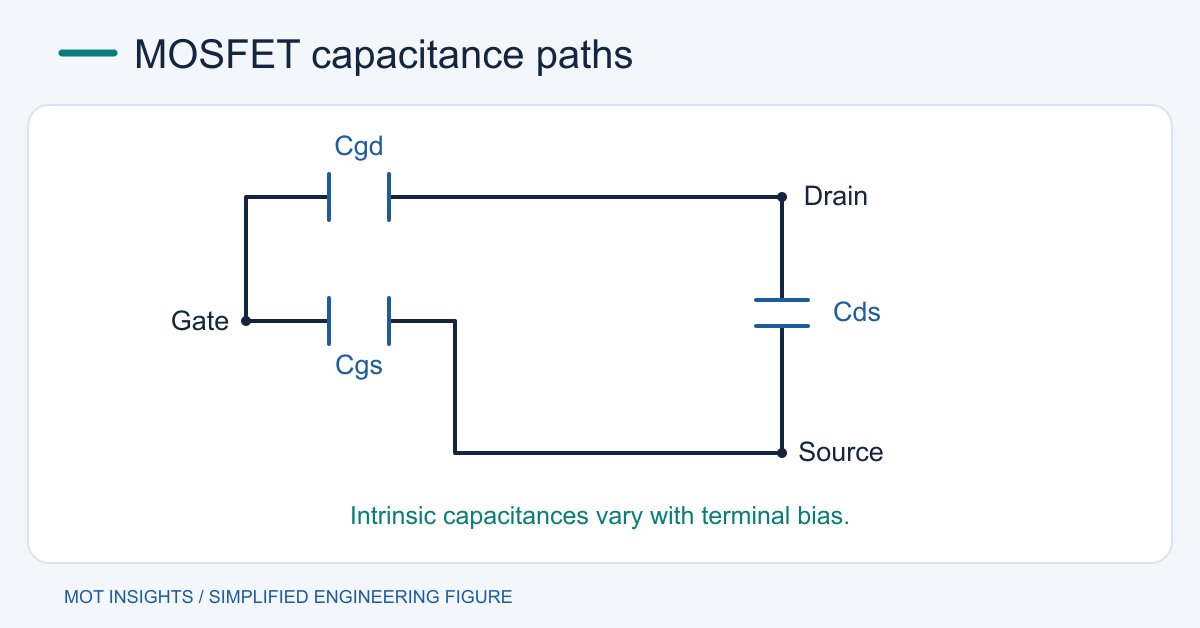
Identify which capacitance is involved
The usual small-signal datasheet relationships are Ciss = Cgs + Cgd, Coss = Cds + Cgd, and Crss = Cgd, under the manufacturer’s measurement conventions. The listed values depend on bias and frequency. Drain-related capacitances vary strongly with VDS. Use the capacitance curves to understand trends, and use charge or energy curves for a large voltage excursion. The gate capacitance guide explains why the measured value changes with conditions.
For hard switching, compare Eoss at the actual drain swing. A fixed ½CV² estimate is suitable only when C is approximately constant over that swing. For resonant switching, the charge required to move the switch node during dead time matters as well as stored energy. See MOSFET output capacitance in LLC converters for the resonant case.
Identify the symptom before changing a component
A high gate bump during the opposite switch’s edge points toward Cgd coupling and the off-state gate impedance. The approximate displacement current is Cgd × dVDS/dt in a narrow bias interval. For example, 20 pF at 20 V/ns implies about 0.4 A of instantaneous coupling before nonlinear effects. Gate return inductance and the driver’s sink impedance decide how much VGS rises. Use a short source-referenced loop, separate turn-off resistance where supported and a Miller clamp if the driver provides one.
High-frequency drain ringing often involves package and layout inductance resonating with device and PCB capacitance. Shorten the commutation loop with local bypassing, then compare before-and-after waveforms at the same current. An RC snubber can damp the resonance and add dissipation. Estimate and verify its thermal cost and ensure the waveform stays within voltage limits. The critical switching-loop layout guide illustrates which loop to reduce.
Common-mode noise can also leave through switch-node copper facing a reference plane, heat sink, chassis or cable. Reduce unnecessary switch-node area and route quiet signals away from it. Keep enough copper for current and thermal performance. Place any isolation or clearance boundaries according to the equipment safety design.
Compare complete losses when changing MOSFETs
A smaller die can have lower gate charge and Eoss yet higher RDS(on). Compare conduction loss with hot resistance and RMS current. Compare measured switching energy at relevant line, load and driver settings. A lower Qgd part may switch faster with the same resistor, increasing overshoot or EMI. Retune the gate network and check margins again. Reserve negative off bias for cases supported by the device and driver.
Verify at the actual switching node
Measure the gate and drain directly at the package with probes rated for differential and common-mode conditions. Long leads add inductance and a probe can change the capacitance of a sensitive node. Compare the two switching edges, test light load and maximum current, and repeat hot. Record loss or EMI changes together with the gate overshoot and drain stress. Compare MOT power MOSFETs using equivalent test voltages and charge conditions.