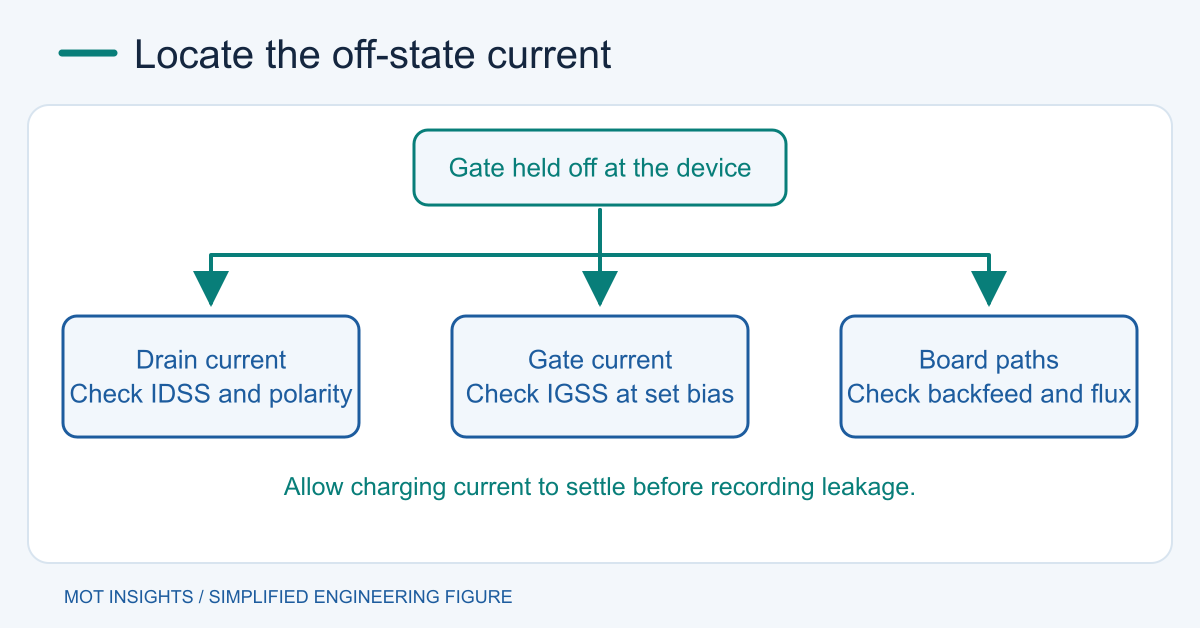
Reduce MOSFET off-state leakage by identifying its path first. Verify gate-to-source voltage at the device, check whether the body diode is forward-biased, then distinguish drain leakage, gate leakage and current through the board or connected loads. Compare the device’s maximum leakage at the actual drain voltage and temperature with the allowed standby or hold-up current.
Read the leakage specifications separately
IDSS is drain-to-source leakage at a specified drain bias, usually with VGS = 0 V. IGSS is gate leakage at a specified positive or negative gate bias with the other terminals connected as stated. They describe different paths. Neither figure includes a pull-up resistor, protection network, PCB contamination or a load powered through another connector.
Use the data sheet’s temperature and voltage conditions when setting a budget. A room-temperature typical reading can be far below the guaranteed hot limit. Also check test polarity. The intrinsic diode in a conventional silicon MOSFET can pass substantial current under the opposite terminal polarity. Review body-diode conduction to distinguish that behavior from off-state leakage.
Check that the gate actually stays off
Measure VGS between the package terminals through startup, steady state and shutdown. An unpowered driver can become high impedance, letting charge remain on the gate. An adjacent switching node can couple current into it through Cgd and produce short bursts of channel conduction. A DC meter can average those bursts into an apparent leakage current.
A source-referenced gate pull resistor provides a defined state during controller reset. Check its value against driver leakage and the circuit’s desired off time. For repetitive dV/dt turn-on, improve the return path and evaluate a stronger sink or Miller clamp. Observe the allowed gate limits for the exact device. The dV/dt protection guide covers the dynamic case.
Measure device and board paths independently
Use a current-limited source and known terminal bias. Tie gate to source when measuring IDSS, use the correct drain polarity, and allow capacitive charging and instrument settling to finish. At microamp or lower levels, measure fixture leakage first. For sensitive measurements, use shielding, suitable guarding, clean insulators and a meter range that can resolve the target. Keep temperature stable and repeat the measurement after thermal soak.
If the board current is high but an isolated part meets specification, check flux residue, moisture, damaged connectors and signal pins that can feed the rail. Disconnect candidate branches systematically. If leakage persists on the removed device, compare drain and gate tests with a known-good part. Unexpected gate leakage after an electrical event warrants checking driver overshoot and oxide stress. Use the gate protection guide for related failure mechanisms.
Convert standby limits into part requirements
For a 100 µF hold-up capacitor allowed to drop 0.5 V over 10 s, the total constant-current budget is CΔV/t = 5 µA. Capacitor self-leakage and the downstream standby load consume part of that allowance. Allocate the remainder to switching devices and other paths using their worst-case hot specifications. If the off-state differential voltage varies over the discharge, measure the actual decay or integrate the voltage-dependent current.
When the load can be driven from either side, a single MOSFET cannot block both directions because of its diode. An appropriately controlled back-to-back pair can provide bidirectional blocking in its off state, with each device’s leakage and gate network still included. If power can arrive through a signal cable, isolate that path separately.
Prioritize a device with a guaranteed leakage limit at the intended voltage and temperature. Compare power MOSFET options using the same bias conditions and check that the lower-leakage candidate still meets on-loss, switching and SOA requirements.