PART 01
/ /
Fence barrier on MOSFET.
Central role in
/ /

In a direct power-driven circuit, MOSFET, as a power switch, has an equivalent electrical capacity (Ciss = Cgd+Cgs) between the fence and the source pole, and the main functions of the grid barrier (Rg) include:
1. Limiting grid-driven currents: preventing the export of large currents by drive chips from damaging the MOSFET fence polar oxidation layer (usually not exceeding ±20V)
2. Control of the number of switches: Change the extreme charge/discharge speed of the fence by regulating the Rg barrier, affecting the opening and closing times of MOSFET
3. Repression of the extreme convulsions of the fence: the parasitic sense and the electric capacity in the polar circuits of the fence form the LC to optimize the VGS wave shape
4. Reduction of EMI electromagnetic interference: a reasonable switch speed can reduce radiation interference from di/dt and dv/dt

PART 02
/ /
Selecting key parameters for barrier resistance
with calculation method
/ /
Core parameter considerations
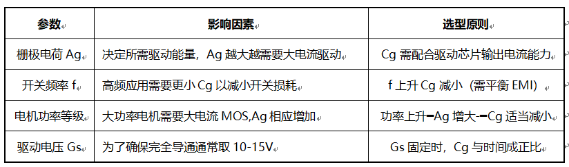
Formula
The grid calculates the current formula in extremely average terms:
Ig avg = Ag x f sw
(Qg: MOSFET grid total charge, f sw: switch frequency)
2. Preliminary estimates of barrier resistance:
Rg Min = (V drive r-Vgsth)/Ig max
(V driver: drive voltage, Vgs th: fence threshold voltage, Ig max: drive chip maximum output current)
3. Opening time and Rg relationship:
t rise ≈2. 2 x Rg x Ciss
t fall ≈2. 2 x Rg x Coss
(t rise: opening time, t fall: off time, Ciss: Enter the cape, Coss: Output cape)


PART 03
/ /
Optimization strategy for VGS wave-shaped distortions
/ /
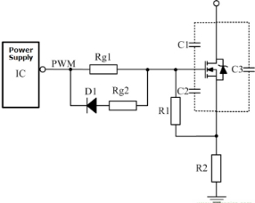
1. Fence barrier optimization:
Detachment barrier electrical resistance (open Rg on ≠ off Rg off)
Recommendation: Rg on < Rg off (accelerated opening, cut off to reduce EMI)
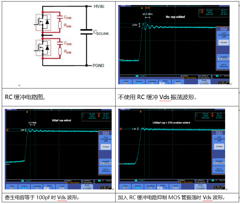
RC buffer circuits
The RC network between the fence and the source pole
Effects: high frequency oscillation inhibited and wave smoother improved degrees
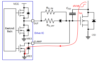
3. Driver chip selection
Select the drive core with Miller's plier function Snippets
Ensure that driver chip output resists match Rg
PCB layout optimization:
Reduction in the length of the fence ' s polar-driven circuit line (< 5 cm)
Use ground floor to reduce parasitic senses
Avoid the parallels between the polar line and the power circuit. Line
(concluded)