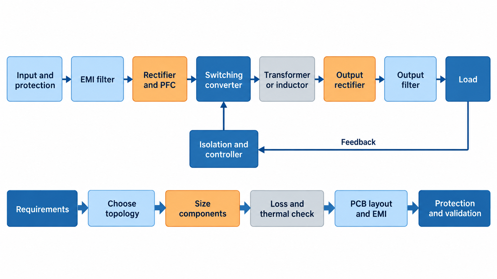
To design a switch-mode power supply, first define the complete input, output, isolation, transient, thermal, mechanical, and regulatory requirements. Then choose the topology and switching frequency, calculate the power stage and magnetics, select components with margin, design the control loop and protection, lay out the PCB around the high-frequency current loops, and validate the prototype across normal and fault conditions.
SMPS design is an iterative engineering process, not a single formula. Topology affects device stress, magnetics, control behavior, EMI, cost, and layout. Component choices change the optimum switching frequency, while layout parasitics change the waveforms used to estimate loss. A successful design closes this loop with measurements.
1. Write the power-supply specification
Record minimum, nominal, and maximum input voltage, including surge, dropout, and source impedance. Define output voltage, continuous current, peak current, allowable ripple, line and load regulation, transient deviation, startup time, hold-up time, and permitted overshoot. State whether the output may sink current or must support bidirectional power flow.
Add the operating and storage temperature range, altitude, cooling method, acoustic limits, size, mass, connector, and cost goals. Decide whether input-to-output isolation is required and, if so, whether it is functional, basic, reinforced, or another class defined by the relevant product standard. Identify efficiency, standby power, power-factor, conducted-emissions, radiated-emissions, immunity, and safety targets.
If the architecture is unfamiliar, read what a switching power supply is before selecting parts. A clear specification prevents a low-cost non-isolated converter from becoming an unsafe answer to an isolated application.
2. Select the topology
For a non-isolated DC conversion, a buck steps voltage down, a boost steps it up, and buck-boost-derived circuits can handle an output above or below the input. Synchronous rectification improves efficiency at low output voltage and high current but adds gate timing and control complexity.
For isolated conversion, flyback is common at lower power because it uses one magnetic component to store and transfer energy. Forward, active-clamp forward, push-pull, half-bridge, full-bridge, phase-shifted full-bridge, and LLC converters serve progressively different power, efficiency, regulation, and switching-stress needs. There is no universal wattage boundary; input range, output voltage, thermal limits, magnetics, switching frequency, and controller ecosystem all matter.
For offline AC-DC equipment, the front end may also need a fuse, surge limiter, inrush control, EMI filter, bridge rectifier, bulk capacitor, and power-factor-correction stage. The article on how many diodes a bridge rectifier uses explains the basic full-wave input stage.
3. Choose switching frequency and operating mode
Higher frequency can shrink inductors, transformers, and capacitors, but it increases switching loss, gate-drive loss, magnetic core loss, EMI, and sensitivity to layout parasitics. Lower frequency often improves efficiency but requires larger energy-storage parts. Select frequency after estimating the total system tradeoff rather than optimizing a single component.
Continuous-conduction, discontinuous-conduction, boundary, valley-switching, zero-voltage-switching, and resonant modes each change peak current, RMS current, control law, and EMI. Controller availability and proven reference designs can narrow the choice. Check the minimum on-time, maximum duty cycle, slope compensation, current-sense range, startup method, burst mode, and synchronization needs.
4. Calculate the power stage
Use the worst input and load corners to calculate duty cycle, inductor or transformer current, peak switch voltage, diode or synchronous-switch stress, capacitor RMS current, and output ripple. Include leakage inductance, rectifier recovery, dead time, tolerance, and transient overshoot rather than selecting parts exactly at ideal equations.
Choose MOSFET voltage rating with margin above the measured and modeled peak drain voltage. Compare hot RDS(on), gate charge, output capacitance, reverse recovery, package inductance, thermal resistance, and safe operating area. A low headline resistance can be a poor choice if its capacitance creates excessive switching loss. The guide to how a MOSFET works provides the device background behind these tradeoffs.
Select rectifiers from repetitive voltage, average and peak current, forward loss, reverse leakage, recovery, junction temperature, and surge requirements. At low output voltages, synchronous MOSFETs may replace diodes. At high voltage or high frequency, silicon-carbide diodes or MOSFETs may reduce switching loss, but the gate drive and layout must suit their edge rates.
5. Design the magnetics
For an inductor, choose ripple-current target, inductance, peak current, saturation margin, winding resistance, core material, core loss, temperature rise, and fringing-field management. For an isolated transformer, add turns ratio, volt-seconds, flux density, core geometry, primary inductance, leakage inductance, insulation system, creepage, clearance, shielding, and interwinding capacitance.
Magnetics loss combines copper loss and frequency-dependent core loss. Skin and proximity effects can make AC winding resistance much higher than its DC value. Litz wire, foil, interleaving, or sectional winding can help, but each choice changes capacitance and manufacturability. Validate the finished magnetic component, not only the core calculation.
6. Select input and output capacitors
Capacitors must withstand voltage, ripple current, temperature, lifetime, and transient energy. ESR creates ripple and heat; ESL limits high-frequency performance. Combine bulk capacitors with ceramic or film parts where appropriate, but check ceramic capacitance loss under DC bias and the possibility that very low ESR alters control-loop damping.
Place local high-frequency capacitors directly across the commutation loop. Large bulk capacitance farther away cannot replace a small, low-inductance ceramic or film capacitor at the switching stage.
7. Design feedback and loop compensation
Choose voltage-mode, peak-current-mode, average-current-mode, hysteretic, constant-on-time, digital, or resonant control to match the topology and performance target. Model the power stage, compensator, sampling effects, right-half-plane zero where applicable, output capacitor, ESR zero, load range, and delay.
Set crossover frequency and phase margin from measured or validated plant behavior. Test at minimum and maximum input, light and heavy load, and operating-mode boundaries. A stable nominal simulation does not prove the converter is stable with component tolerance, current limiting, burst transitions, or a different load impedance.
8. Add protection before layout
Plan input undervoltage and overvoltage lockout, output overvoltage, cycle-by-cycle current limit, short-circuit response, overload timing, overtemperature protection, reverse-polarity protection, inrush limiting, brownout behavior, and safe restart. Decide whether a fault latches, hiccups, folds back, or retries, and verify that the response protects the switch, rectifier, magnetics, wiring, and load.
For mains equipment, use appropriately rated fuses, surge protective parts, X and Y capacitors, isolation components, and spacing required by the actual standard and pollution degree. Do not treat a bench fuse as the complete safety system.
9. Estimate loss and temperature
Create a loss budget for every operating corner: MOSFET conduction and switching, rectifier loss, magnetic copper and core loss, capacitor ESR, gate drive, current sense, controller, snubbers, bleeders, and auxiliary supply. The sum should reconcile with the expected efficiency.
Convert loss into junction and hot-spot temperatures using the real thermal paths, interface materials, board copper, airflow, enclosure, altitude, and ambient temperature. Use the article on MOSFET heatsink sizing when discrete switches need external cooling.
10. Lay out the PCB by current loop
Identify the high-di/dt loop that conducts during each switching state. Keep the switch, rectifier or synchronous MOSFET, and high-frequency capacitor close together with a small loop area. Keep the switch node compact because its high dV/dt drives capacitive noise into nearby conductors.
Separate quiet analog ground from the noisy power path and join them at the controller’s intended point. Route gate and source return as a tight pair. Use Kelvin sensing for current shunts and output feedback. Keep feedback away from the switch node, transformer gap, and gate traces. Observe creepage and clearance without routing copper beneath isolation barriers.
11. Control ringing and EMI
Ringing usually comes from parasitic inductance resonating with device capacitance. Improve layout before adding a snubber. Then measure the ringing frequency and tune an RC, RCD, clamp, or active-clamp network from real hardware. Excessive snubbing hides a poor layout and wastes power.
Design the input filter with the source and converter impedance in mind so it does not destabilize the control loop. Separate common-mode and differential-mode noise mechanisms. Use short return paths, shield or screen magnetics where justified, and provide a controlled chassis connection. Pre-compliance testing early in the prototype cycle is cheaper than a late redesign.
12. Prototype and validate
- Inspect the unpowered board, resistance, polarity, isolation gap, and component orientation.
- Start from a current-limited source at reduced voltage where the topology permits.
- Check bias rails, gate waveforms, duty cycle, dead time, and startup sequence before full load.
- Increase input voltage and load in controlled steps while monitoring temperature and stress.
- Measure efficiency, ripple, regulation, transient response, loop gain, startup, shutdown, and hold-up.
- Test short circuit, overload, open feedback, brownout, output prebias, fan failure, and thermal protection as applicable.
- Run conducted and radiated EMI pre-compliance tests with production cables and enclosure.
- Repeat critical tests at temperature and with worst-case component tolerance.
Use properly rated isolated probes, differential probes, current probes, and safe test fixtures. Offline converters contain lethal voltage and stored energy even after disconnection. Qualified personnel should perform high-voltage development inside controlled laboratory procedures.
Frequently asked questions
Which SMPS topology is best?
The best topology is the one that meets conversion ratio, isolation, power, efficiency, transient, size, EMI, safety, and cost requirements with acceptable design risk.
Can I copy a reference design?
A reference design is an excellent starting point when its input, output, layout, magnetics, thermal conditions, and standards closely match yours. Recalculate and validate every change.
Why does an SMPS work on the bench but fail EMI?
Bench operation proves basic conversion, not electromagnetic compatibility. Loop area, switch-node capacitance, cable currents, common-mode paths, enclosure, and probing can dominate emissions.
Do I need an oscilloscope?
Yes for serious development. A multimeter cannot reveal gate ringing, drain overshoot, loop instability, switching loss, startup stress, or many intermittent faults.