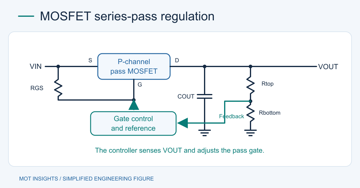
A MOSFET can act as the series pass element in a linear voltage regulator. A reference, output divider and error amplifier adjust its gate voltage to hold the output at a set point. The device carries load current while dropping the difference between input and output voltage, so safe operating area (SOA), heat dissipation and feedback stability govern the design.
How feedback sets the output
For a high-side P-channel pass device, connect its source to the input and its drain to the output. The controller pulls the gate farther below the source when more conduction is needed and brings it back toward the source to reduce conduction. It must keep gate-to-source voltage within the device rating over the full input range and during transients. A resistor from gate to source can hold the device off when the pull-down driver is inactive. A practical circuit also needs a defined startup state and an appropriately rated driver. Driving a P-channel MOSFET
Place Rtop between the output and the feedback node and Rbottom between feedback and ground. With negligible input bias current and operation inside the control loop’s valid range, Vout ≈ Vref × (1 + Rtop ÷ Rbottom). A 1.25 V reference, 30 kΩ top resistor and 10 kΩ bottom resistor yield a nominal 5.0 V. Reference accuracy, resistor tolerance, bias current and ground voltage all enter the error budget. Sense at the node that needs regulation.
An N-channel pass element is another option. In the usual high-side configuration its gate needs headroom above the output, and low dropout near the input often requires an auxiliary gate rail or a purpose-designed controller. A fixed gate with a source-follower connection can produce a rough output offset, but VGS changes with load, temperature and device variation. Include feedback for a controlled set point and line and load regulation.
Calculate heat and check the operating area
Suppose the output is 5 V at 0.4 A from a 12 V rail. At nominal conditions the pass element drops 7 V and dissipates about 2.8 W, excluding drive and divider consumption. With an actual effective junction-to-ambient thermal resistance of 25 °C/W for the assembly, the first-pass rise is about 70 °C. At 45 °C local ambient, that estimates 115 °C junction temperature. Higher input, heavier load or poor airflow can raise it further.
Check 7 V and 0.4 A against the MOSFET’s applicable DC SOA, derated for the expected case temperature. Low on-resistance and high headline current do not establish DC linear-mode capability. At partially enhanced gate voltages, localized heating can limit the transistor before simple package power calculations predict failure. Confirm both the SOA curve and the design’s thermal limits. At startup or during a short, VDS can approach the full input while current is limited. Foldback, a timer or latch-off may be needed. For example, a short at a 0.4 A constant limit on 12 V dissipates about 4.8 W in the pass device until protection acts. Reading a MOSFET SOA chart
Check dropout, stability and reverse current
Dropout is the minimum input-to-output headroom needed to hold regulation under specified load and temperature. Once the amplifier runs out of gate drive, the available channel resistance and circuit wiring constrain the minimum drop. Evaluate a hot device with the worst-case drive available. At the other end of the input range, compare power loss with the system’s thermal budget. Comparing linear and switching supplies
The gate capacitance, driver impedance, output capacitance, capacitor ESR and load change the feedback loop dynamics. Use the regulator controller’s compensation guidance and validate load-step response across input voltage, load, components and temperature. Check startup and shutdown separately. In a P-channel high-side arrangement the body diode can allow reverse current from output to input when the output remains powered and the input collapses. Include a reverse blocking arrangement when the system needs isolation between rails. MOSFET body-diode behavior
Frequently asked questions
Can a switching MOSFET run continuously in a linear regulator?
It can when the manufacturer specifies a suitable DC SOA and the operating point, temperature and protection fit it. Use a part characterized for linear operation when the regulator must sustain significant voltage and current simultaneously.
Is a discrete MOSFET always better than an integrated regulator?
An external pass transistor gives freedom over package and heat dissipation. An integrated regulator may already provide compensation, current limiting and thermal shutdown. Compare the required current, dropout, fault behavior and board area.
For pass-device selection, bring the steady-state and startup stress points, case-temperature target and available gate voltage to the MOT applications team.