Protect a MOSFET gate by keeping gate-to-source voltage inside its positive and negative limits during drive, switching transients, startup, shutdown, and handling. The oxide is thin and can be damaged by overvoltage or electrostatic discharge. A gate clamp helps, but layout, driver behavior, pull-down, source inductance, and drain dV/dt determine what the device actually sees.
Measure VGS at the gate and source pins. A clean waveform at the driver connector can coexist with damaging pin-level spikes.
Set a safe normal drive voltage
Choose the driver supply from the resistance or performance specifications and leave margin below absolute maximum VGS. Include regulator tolerance, bootstrap overshoot, transformer ringing, Miller coupling, and negative source bounce. Gate absolute maximum is a survival limit, not a recommended operating target.
The discussion of gate-oxide margin explains why added drive beyond the plateau may offer little benefit.
Add a close gate-to-source clamp
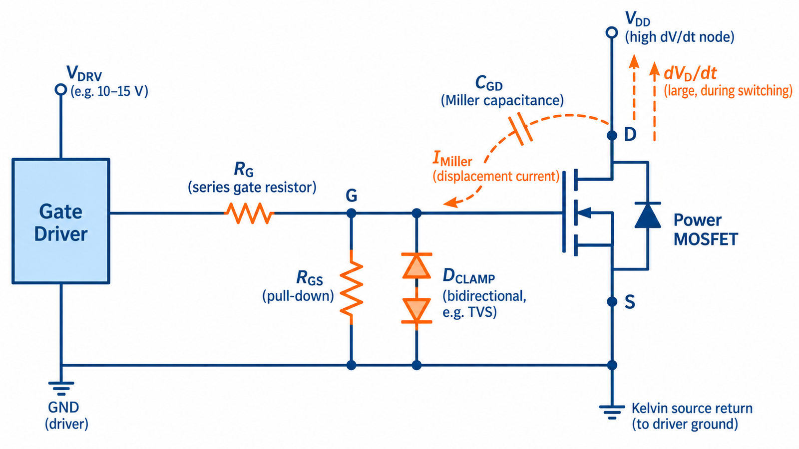
A Zener or dedicated gate protector can limit positive VGS; a bidirectional arrangement or diode may be needed for negative stress. Select clamp tolerance, dynamic voltage at actual pulse current, leakage, capacitance, pulse energy, and temperature. Place it next to the MOSFET, not at a distant driver.
Return the clamp to the device’s source or Kelvin source so power-loop voltage does not add to the protected voltage.
Define the off state
A gate-to-source resistor discharges the gate and holds it off when the driver is high impedance. Size it against driver leakage, Miller current, dV/dt, and acceptable standby current. For a high-side device, the resistor must connect to its moving source, not system ground.
Confirm off-state behavior during MCU reset, cable disconnection, undervoltage lockout, and power sequencing.
Control Miller turn-on
Drain dV/dt sends current through CGD. If the turn-off path impedance is too high, VGS can cross threshold and cause shoot-through. Use a strong sink, smaller turn-off resistance, Miller clamp, negative bias where justified, and a Kelvin source. Lower switching-loop inductance reduces source bounce.
See protection from dV/dt for a complete bridge-oriented treatment.
Use the gate resistor deliberately
The series resistor limits peak driver current, damps the gate loop, and adjusts edge speed. It should be placed near the gate so the trace between resistor and device is short. Too little resistance can excite ringing and EMI; too much increases switching loss and susceptibility to Miller turn-on. Separate turn-on and turn-off paths may provide better control.
Validate with the gate-resistor tuning method.
Protect handling and external interfaces
Use grounded work surfaces, wrist straps, antistatic packaging, and controlled assembly procedures. A gate exposed on a connector may need a dedicated ESD protector chosen for capacitance and clamp performance. Series resistance near the interface can limit surge current, but must not make switching unacceptably slow.
After any suspected overstress, check gate leakage and switching behavior; oxide damage can be latent rather than a clean short.
Turn the answer into a robust MOSFET design
For How to Protect a MOSFET Gate, create an operating-state table before choosing a device or protection value. Include off, startup, steady on, PWM transitions, shutdown, reverse current, load connection, controller reset, brownout, open load, overload, and short circuit. For each state, write the expected VGS, VDS, current, duration, repetition, and starting temperature. This exposes short but severe events that an average-current calculation hides.
Next, compare the table with guaranteed data-sheet limits and characterized curves. Use voltage margin for supply tolerance and ringing; use RDS(on) at the actual gate voltage and hot junction; use total gate charge and Miller charge for driver sizing; and use DC or pulsed SOA for intervals where voltage and current coexist. Include package, PCB copper, interface material, airflow, connector, and source-return inductance in the model. A transistor cannot be evaluated separately from its commutation path and gate loop.
Build a staged test plan that begins with limited available energy. Capture gate-to-source voltage at the pins, drain-source voltage, current, and temperature while changing one stress at a time. Repeat enough cycles to reveal cumulative heating and recovery behavior. Define pass limits before looking at the waveform, preserve oscilloscope files, and record device lot, ambient, probe method, and firmware revision. If measured peaks approach an absolute maximum, redesign for margin rather than accepting the result because one prototype survived.
Practical validation checklist
Validate at the worst credible supply voltage, load current, switching frequency, ambient temperature, and fault condition. Measure gate-to-source voltage at the device pins, drain-to-source voltage with adequate bandwidth, current, case temperature, and—when power or pulses are significant—estimated junction temperature. Account for probe ground inductance and avoid interpreting ringing created by the measurement setup as circuit behavior.
Compare every result with the data-sheet safe operating area, absolute maximum ratings, transient thermal impedance, and temperature-dependent curves. Test startup, shutdown, load connection, stalled or shorted load, controller brownout, and repeated operation. The guides to reading MOSFET safe operating area and MOSFET thermal calculation provide useful companion checks.
Frequently asked questions
What Zener voltage should protect a 20 V gate?
Choose from the normal drive, clamp tolerance, dynamic voltage, pulse current, and desired margin; do not place the clamp at the 20 V absolute maximum.
Can a gate resistor protect against ESD?
It can limit current, but dedicated ESD handling and a suitable close clamp may still be required.
Why does VGS go negative at turn-off?
Common-source inductance and gate-loop ringing can drive the source above the gate; improve layout, return path, damping, and clamp design.
Is the internal gate-source resistor enough?
Many MOSFETs have no useful internal pull-down. Use the data sheet and add an external resistor when a defined off state is required.