
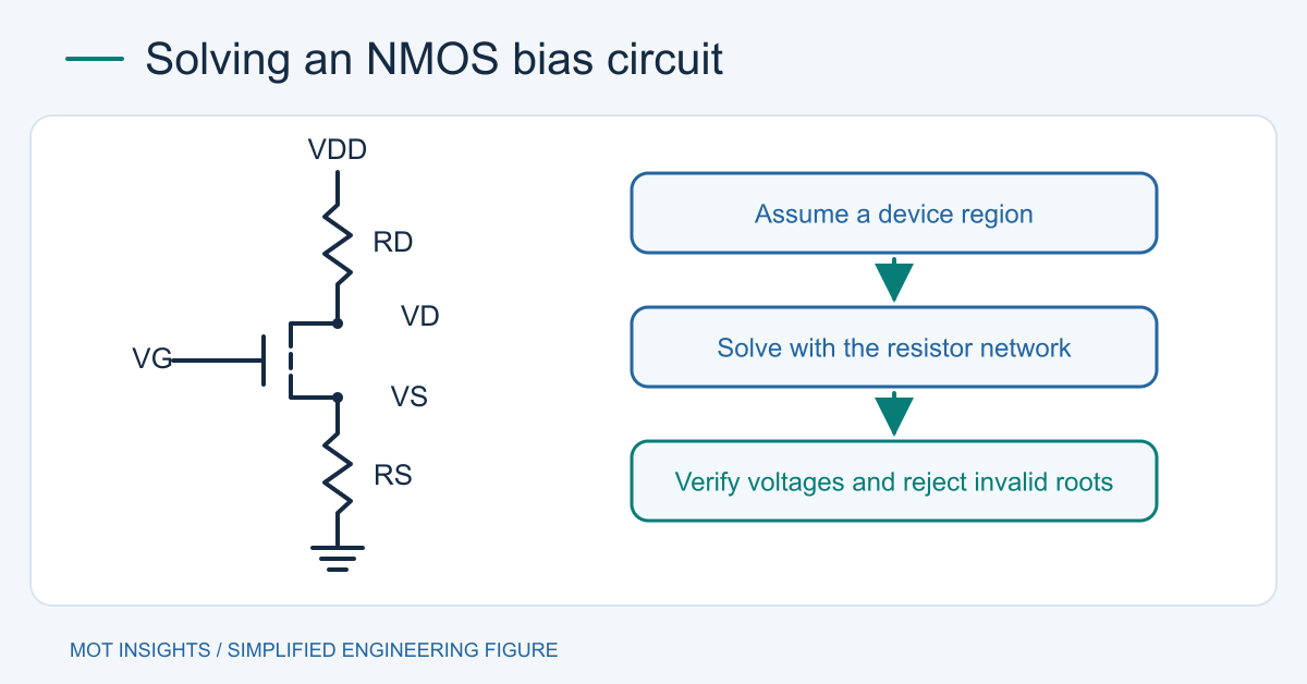
Solve a MOSFET DC circuit by writing its node voltages from the resistor network, assuming a transistor operating region, and solving the corresponding current equation. Substitute each candidate current back into the circuit and check the region inequalities. If the solution violates them, choose the appropriate model and solve again. This gives a valid bias point for the stated device approximation.
Write the circuit relationships first
Consider an enhancement NMOS with a resistor RD to VDD, a resistor RS to ground and a stiff gate voltage VG. Ignore DC gate current, body effect and channel-length modulation for the examples. Use this sign convention: VGS = VG − VS, VDS = VD − VS, and positive ID enters the drain. With no other DC current branches, VS = ID × RS and VD = VDD − ID × RD. Therefore VDS = VDD − ID × (RD + RS).
These equations describe the external circuit. The device equation supplies the additional relationship. If a bias divider supplies the gate, compute its unloaded voltage as a first estimate and account for leakage if the divider is high impedance. If an output load shares the drain, write KCL there instead of assuming RD carries only ID. MOSFET drain-current analysis
State the model and test the assumption
For an ideal long-channel NMOS with positive VDS, define overdrive VOV = VGS − VTH and use k in amperes per volt squared. Cutoff gives ID ≈ 0 when VOV ≤ 0. In triode operation, 0 ≤ VDS < VOV and ID = k(VOV × VDS − VDS²/2). In saturation, VDS ≥ VOV > 0 and ID = k × VOV²/2. Some references absorb the factor of two into a different parameter, so keep one convention through the calculation.
Start with cutoff if the open-channel circuit makes VGS small. If the result gives VGS above threshold, test a conducting region. Reject roots that require a negative overdrive under the saturation assumption, violate the assumed drain polarity, or cannot exist with the given rails. The operating-region guide explains the physical meaning of these inequalities.
Example 1. Find the bias with a source resistor
Assume VDD = 9 V, VG = 4 V, RD = 1 kΩ, RS = 1 kΩ, VTH = 1 V and k = 2 mA/V². Use i as the numerical drain current in mA, so each 1 kΩ resistor drops i volts. Then VOV = 3 − i and VDS = 9 − 2i, both in volts. The assumed saturation equation becomes i = (3 − i)². Solving yields i = (7 ± √13)/2, or approximately 1.70 mA and 5.30 mA.
At 5.30 mA the assumed overdrive is negative, and VDS would be negative as well. At 1.70 mA the overdrive is about 1.30 V and VDS is about 5.61 V. Both saturation inequalities hold at the smaller root. The DC voltages are VS ≈ 1.70 V and VD ≈ 7.30 V with rounding. The self-bias resistor lowers VGS as current rises, so using the gate voltage alone would overpredict the current.
Example 2. Recalculate when saturation fails
Keep the same transistor model, set RS = 0, RD = 1 kΩ, VDD = 2 V and VG = 3 V. Here VOV = 2 V. The saturation equation predicts 4 mA, which would require a drain voltage of −2 V. Use triode instead. Let v be the numerical VDS in volts. The resistor supplies 2 − v mA, and the transistor equation gives 4v − v² mA. Equating the two gives v² − 5v + 2 = 0.
The two roots are about 0.438 V and 4.562 V. Only the first root is below both VOV and the supply voltage. This gives ID ≈ 1.56 mA and confirms triode operation. A load-line sketch gives the same result as the algebra. The resistor’s straight line intersects the actual device curve at the operating point, so a graphical intersection can also replace the ideal equations when datasheet curves are available.
Transfer the result to a real circuit
For a PMOS, use source-referenced VSG and VSD with the appropriate current direction and threshold magnitude. For a discrete power switch operating near the on state, calculate drop using the specified RDS(on) at the real gate voltage and temperature. A textbook k and threshold estimate can produce very different current from the selected device. In linear service, calculate VDS × ID and verify DC or transient safe operating area.
Build a low-voltage, current-limited test if the bias is important. Measure VG, VD and VS at the package and recalculate VGS and VDS. Sweep expected threshold, temperature and supply variation in the model. The small-signal MOSFET circuit guide shows how this DC point becomes the starting point for gain analysis. For device data and hot resistance, compare MOT MOSFET options.