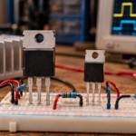
Test a depletion-mode MOSFET by confirming that it conducts with the gate tied to the source, then applying the specified opposite-polarity gate voltage to reduce or stop drain current. For an N-channel depletion device, zero VGS normally produces conduction and a negative VGS turns it toward off. A P-channel device uses opposite polarities.
That behavior is the reverse of the familiar enhancement-mode power MOSFET test. Always obtain the exact data sheet first because pinout, channel type, current range, gate limits, and off voltage vary widely.
Identify the device before connecting power
Read the full marking and verify the package drawing. Do not assume that two TO-92, SOT-89, or TO-220 parts share the same gate, drain, and source order. Note VDS, IDSS, VGS(off), RDS(on), maximum gate voltage, and test conditions. Some depletion devices are designed as current regulators rather than low-resistance switches.
If the part is still in circuit, parallel resistors, diodes, transformer windings, and controller pins can dominate measurements. Remove the device or lift a lead when safe diagnosis requires isolation.
Perform unpowered short checks
Disconnect all power and discharge capacitors. With a multimeter, check for a near-zero short between gate and source or gate and drain in both polarities. The insulated gate should normally show very high resistance, although meter range, protection components, contamination, and in-circuit paths affect the result. Check drain-to-source in both directions and account for any body diode.
A hard short is evidence of failure, but an apparently open gate does not prove the transistor is healthy. The channel is normally present at zero gate bias.
Build a current-limited zero-bias test
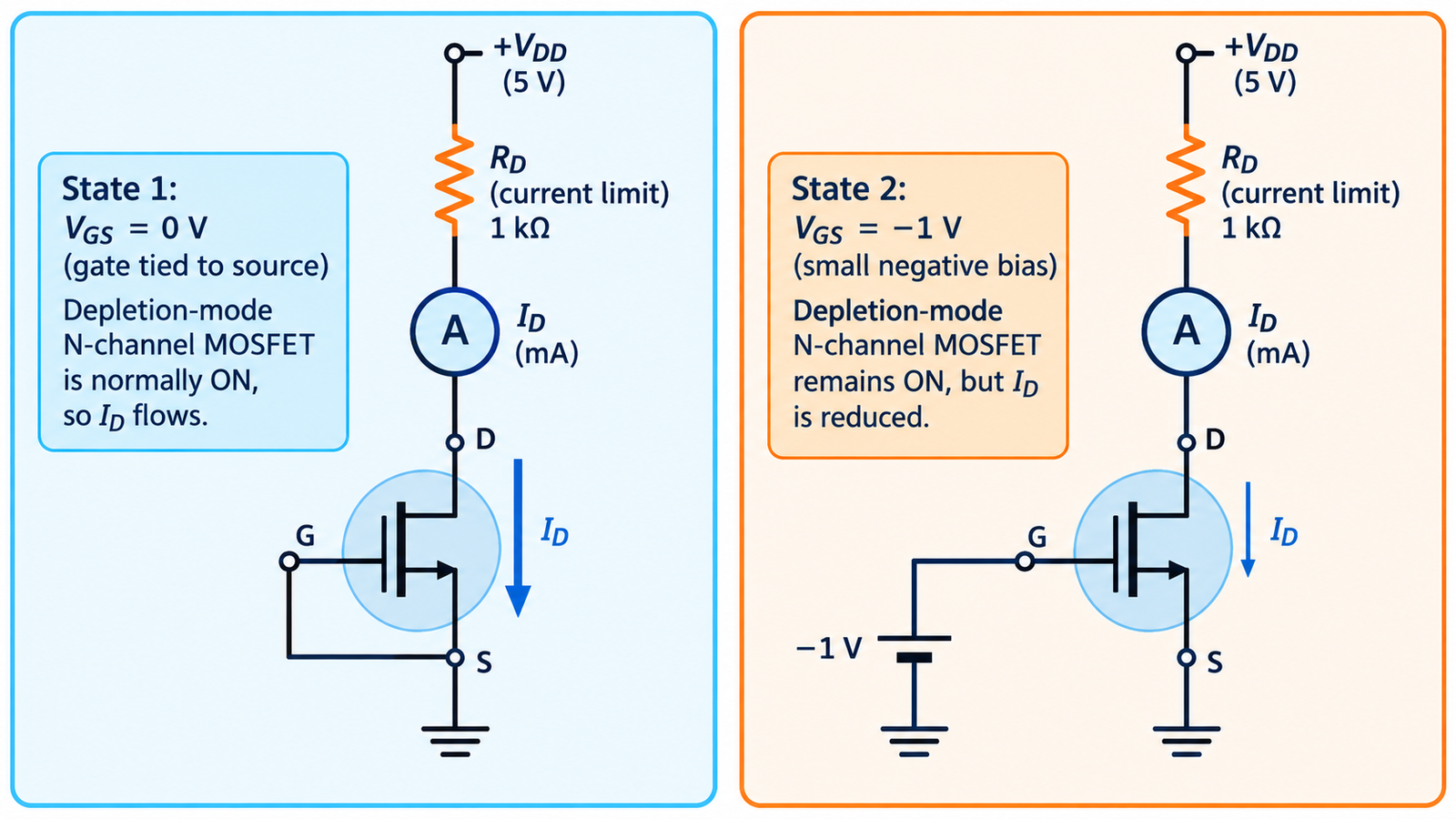
Use a low DC supply well below the device’s rating, a series resistor, and an ammeter. For an N-channel device, connect drain to positive through the resistor, source to return, and gate directly to source. Choose the resistor so worst-case current is safe for the MOSFET, supply, and meter. At VGS = 0, a healthy depletion device should conduct according to its transfer and output characteristics.
Do not expect the current to equal a generic value. Compare with the data-sheet IDSS condition and account for device spread and temperature.
Apply gate bias to confirm control
Keep the source as the measurement reference. Apply a small negative gate-to-source voltage to an N-channel depletion MOSFET using an isolated or suitably referenced adjustable source. Increase magnitude gradually without exceeding the gate limit. Drain current should fall as VGS approaches the specified off range. Reverse the polarities for a P-channel device.
The conceptual difference from enhancement mode is clearer after reviewing how a MOSFET channel responds to gate voltage.
Measure on-resistance only at a valid point
If the device data sheet specifies RDS(on) at VGS = 0 or another bias, apply the stated gate voltage and a safe test current. Measure drain-to-source voltage close to the package and calculate R = V/I. Lead and contact resistance can dominate a low-ohmic result, so use Kelvin sensing when necessary. Keep pulses short if the fixture cannot remove heat.
Do not infer high-voltage blocking from a low-voltage bench test. Leakage and breakdown require specialized equipment and safe procedures.
Interpret ambiguous results
No drain current at zero bias may mean an open device, wrong pinout, insufficient meter or supply compliance, a P-channel device connected backward, or a mislabeled enhancement MOSFET. Current that cannot be reduced may indicate a shorted gate, incorrect bias reference, insufficient negative voltage, or channel damage. Compare against a known-good part when possible.
Threshold and off-voltage specifications are ranges, not precision set points. Temperature changes current, so record the test conditions and avoid heating the device during diagnosis.
Practical design review
Use a fixture with a physical current limit, series resistor, clearly labeled polarity, and a gate-source clamp if an adjustable supply could exceed the rating. Power the drain and gate sources in a sequence that never leaves the device exposed to destructive current. Avoid touching the gate lead; electrostatic charge can alter the reading or damage the oxide. For high-voltage depletion parts, keep this basic functional test at low voltage.
After a device passes, evaluate it in the intended operating region. Confirm current at zero bias, transfer behavior, hot RDS(on), leakage, power dissipation, and safe operating area. The broader procedures in testing a P-channel MOSFET and understanding MOSFET applications help distinguish a functional check from full characterization.
Document supply voltage, series resistance, measured gate bias, drain current, package temperature, meter model, and pin orientation. Repeating the test from that record is more useful than labeling the part simply good or bad. If a replacement sits in a precision current source, characterize several samples because the zero-bias current and off voltage can vary substantially.
Frequently asked questions
Is a depletion-mode MOSFET normally on?
Yes. A depletion MOSFET has a conducting channel at zero gate-to-source voltage. Gate bias of the appropriate opposite polarity depletes that channel.
Can I test it with only a multimeter?
A meter can find gross shorts and sometimes show channel conduction, but a current-limited supply and controlled gate bias provide a much clearer functional test.
Why does it conduct after I short gate to source?
That is expected for a depletion-mode device. Shorting gate to source creates VGS = 0, its normally-on condition.
Can I test its breakdown voltage on a bench?
Not with an ordinary low-voltage test. High-voltage leakage and breakdown testing require properly rated equipment, guarding, current limiting, and trained procedures.