Most conventional discrete silicon power MOSFETs have an intrinsic body diode, but “all MOSFETs” is too broad. The diode is a consequence of the device’s body regions and the common practice of connecting body to source. It is obvious and often characterized in vertical power MOSFET data sheets.
Small integrated MOSFETs can have body connections managed by the IC process, and wide-bandgap devices may behave differently. Enhancement-mode GaN transistors, for example, can conduct reverse current without the same silicon p-n body diode or its classic reverse-recovery behavior.
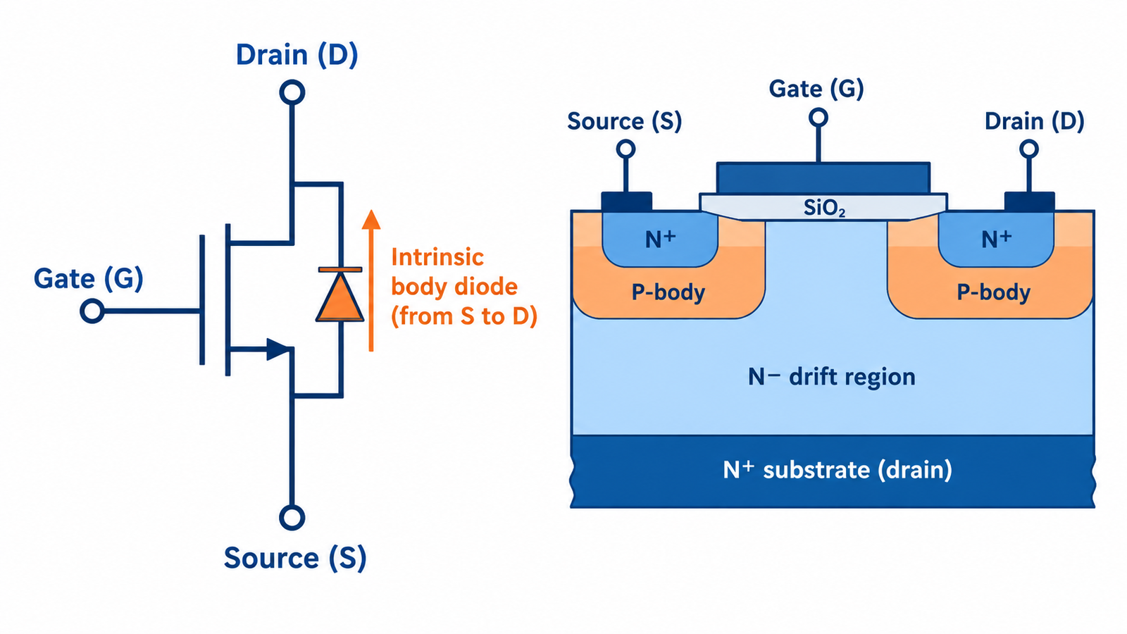
Where the diode comes from
In an N-channel vertical silicon power MOSFET, p-body and n-type drain regions form a p-n junction. With the body tied to source, this appears electrically as a diode between source and drain. For a P-channel device, the orientation reverses. The schematic symbol may show it explicitly, but the physical diode exists even when a simplified symbol omits it.
The foundation in how MOSFETs work explains the gate-controlled channel separately.
What the data sheet specifies
Look for continuous source current, pulsed source current, diode forward voltage, reverse-recovery time, recovered charge, peak reverse-recovery current, and test conditions. Not every manufacturer uses identical terminology. Values depend on current, di/dt, gate state, temperature, and the commutating circuit.
The MOSFET’s impressive drain-current headline does not guarantee that its body diode is efficient or rugged for continuous rectification.
Body-diode conduction during dead time
In a half bridge, load current must continue when both MOSFET channels are briefly off. It may flow through one body diode during dead time. Turning the opposite switch on then commutates the diode, and reverse-recovery current can add loss, ringing, and device stress. Shorter dead time can reduce diode conduction but too little dead time creates shoot-through.
Synchronous control should be tuned with real waveforms and temperature.
Channel reverse conduction can reduce drop
If the gate is driven on while reverse current is present, the MOSFET channel can conduct that current with an approximately resistive drop. This is the basis of synchronous rectification. The body diode may still conduct initially or during timing gaps, and it defines an off-state current path.
The article on bidirectional MOSFET conduction explains why two devices are needed for bidirectional blocking.
Technology exceptions and differences
SiC MOSFETs have a body diode, but its forward voltage and bipolar degradation considerations differ from ordinary silicon devices, and modern generations are characterized for particular uses. GaN HEMTs generally provide reverse conduction through device physics rather than a conventional body diode; their reverse drop depends strongly on gate state and dead time.
Integrated analog switches may expose body terminals differently or use complementary devices to control parasitic paths. Always analyze the actual component.
When to add an external diode
An external Schottky, ultrafast silicon, or SiC diode may reduce forward loss or change commutation behavior, but parasitic inductance and capacitance can prevent it from taking current as expected. In very low-voltage silicon MOSFETs, the body diode can have a lower effective clamp voltage at high current than a remote Schottky once layout is included.
Simulate cautiously, then verify current sharing, reverse recovery, overshoot, and temperature on hardware.
Turn the answer into a robust MOSFET design
For Do All MOSFETs Have Body Diodes?, create an operating-state table before choosing a device or protection value. Include off, startup, steady on, PWM transitions, shutdown, reverse current, load connection, controller reset, brownout, open load, overload, and short circuit. For each state, write the expected VGS, VDS, current, duration, repetition, and starting temperature. This exposes short but severe events that an average-current calculation hides.
Next, compare the table with guaranteed data-sheet limits and characterized curves. Use voltage margin for supply tolerance and ringing; use RDS(on) at the actual gate voltage and hot junction; use total gate charge and Miller charge for driver sizing; and use DC or pulsed SOA for intervals where voltage and current coexist. Include package, PCB copper, interface material, airflow, connector, and source-return inductance in the model. A transistor cannot be evaluated separately from its commutation path and gate loop.
Build a staged test plan that begins with limited available energy. Capture gate-to-source voltage at the pins, drain-source voltage, current, and temperature while changing one stress at a time. Repeat enough cycles to reveal cumulative heating and recovery behavior. Define pass limits before looking at the waveform, preserve oscilloscope files, and record device lot, ambient, probe method, and firmware revision. If measured peaks approach an absolute maximum, redesign for margin rather than accepting the result because one prototype survived.
Practical validation checklist
Validate at the worst credible supply voltage, load current, switching frequency, ambient temperature, and fault condition. Measure gate-to-source voltage at the device pins, drain-to-source voltage with adequate bandwidth, current, case temperature, and—when power or pulses are significant—estimated junction temperature. Account for probe ground inductance and avoid interpreting ringing created by the measurement setup as circuit behavior.
Compare every result with the data-sheet safe operating area, absolute maximum ratings, transient thermal impedance, and temperature-dependent curves. Test startup, shutdown, load connection, stalled or shorted load, controller brownout, and repeated operation. The guides to reading MOSFET safe operating area and MOSFET thermal calculation provide useful companion checks.
Frequently asked questions
Can I remove the MOSFET body diode?
No; it is intrinsic to conventional discrete silicon power-MOSFET structure. Back-to-back devices can block its unwanted path.
Does the body diode conduct when the MOSFET is on?
The channel can carry reverse current with lower drop; actual division depends on gate voltage, current, resistance, and diode voltage.
Do GaN transistors have body diodes?
Enhancement-mode GaN devices do not have the same intrinsic p-n body diode as silicon MOSFETs, although they support reverse conduction.
Is the body diode avalanche rating the same as reverse recovery?
No. Avalanche and reverse recovery describe different events and have different tests and limits.