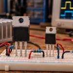
Yes, a MOSFET has a voltage drop. When it is fully enhanced and used as a switch, the dominant channel drop is approximately VDS = ID × RDS(on). That can be millivolts in a well-chosen low-voltage device or several volts when the device is under-driven, hot, overloaded, operating linearly, or blocking current.
The useful question is therefore not whether a drop exists, but how large it becomes in every operating interval. Gate drive, temperature, current waveform, package resistance, reverse conduction, and switching transitions all change the answer.

Calculate the static on-state drop
Start with the data-sheet RDS(on) specified at a gate voltage you can actually deliver. Multiply it by drain current for a first estimate. A 10 mΩ device at 20 A has about 0.20 V channel drop and roughly 4 W conduction loss if that current is continuous. For a pulsed or PWM load, use RMS current for resistive loss rather than blindly multiplying the peak current by duty cycle.
This model applies only when the MOSFET is adequately enhanced. The explanation of how MOSFETs work shows why a gate voltage above threshold is not the same as a low-resistance on state.
Correct RDS(on) for temperature
The front-page resistance is commonly characterized at a 25 °C junction. Silicon power MOSFET channel resistance normally increases with temperature, sometimes substantially. Use the normalized RDS(on)-versus-temperature graph or the maximum hot specification when available. Iterate: estimate loss, calculate junction temperature, update resistance, and repeat until the result converges.
Package leads, bond wires, PCB copper, connectors, and current shunts add voltage that a remote measurement may mistakenly attribute to the silicon. Kelvin-source packages and four-wire measurement help separate channel behavior from interconnect loss.
Gate voltage determines the channel resistance
Use the resistance rating at the stated VGS, not the threshold-voltage line. Threshold is measured at a tiny current and merely indicates the start of channel formation. A standard MOSFET rated at 10 V gate drive may have much higher resistance at 5 V; a logic-level device may be characterized at 4.5 V, 2.5 V, or lower.
Gate-driver droop, source inductance, negative transients, and common-source voltage can reduce the effective gate voltage during a current edge. Measure VGS directly across gate and source pins with appropriate probing.
Account for switching intervals
During turn-on and turn-off, voltage and current overlap. The instantaneous drain-source voltage can be a large fraction of the supply even though the eventual on-state drop is small. Switching energy depends on transition time, frequency, capacitances, gate resistance, circuit inductance, and the commutation partner. Average dissipation can therefore be dominated by transitions rather than conduction.
Use the guidance on tuning a MOSFET gate resistor to balance transition loss, ringing, overshoot, and emissions.
Reverse current and the body diode
If reverse current flows before the channel is enhanced, the intrinsic body diode may conduct with a diode-like forward voltage. When the channel is turned on, many MOSFETs can carry reverse current through the channel with a resistive drop; the exact behavior depends on VGS, current, and device structure. Dead time in a half bridge can make the body-diode interval an important loss term.
Do not treat body-diode current as free. Forward drop, reverse recovery, stored charge, and commutation overshoot can affect efficiency and reliability.
Measure the right voltage
For a DC load, measure from drain pin to source pin after thermal equilibrium and record gate voltage and current. For PWM, use a differential probe or a safe equivalent with adequate common-mode rating and bandwidth. Separate the fully-on plateau from turn-on, turn-off, dead-time, and avalanche intervals. A handheld meter may display only an average that hides damaging peaks.
Repeat at low and high input, minimum and maximum load, hot ambient, and relevant fault conditions. Compare measured loss with the reasons MOSFETs heat up before finalizing cooling.
Turn the answer into a robust MOSFET design
For Do MOSFETs Have a Voltage Drop?, create an operating-state table before choosing a device or protection value. Include off, startup, steady on, PWM transitions, shutdown, reverse current, load connection, controller reset, brownout, open load, overload, and short circuit. For each state, write the expected VGS, VDS, current, duration, repetition, and starting temperature. This exposes short but severe events that an average-current calculation hides.
Next, compare the table with guaranteed data-sheet limits and characterized curves. Use voltage margin for supply tolerance and ringing; use RDS(on) at the actual gate voltage and hot junction; use total gate charge and Miller charge for driver sizing; and use DC or pulsed SOA for intervals where voltage and current coexist. Include package, PCB copper, interface material, airflow, connector, and source-return inductance in the model. A transistor cannot be evaluated separately from its commutation path and gate loop.
Build a staged test plan that begins with limited available energy. Capture gate-to-source voltage at the pins, drain-source voltage, current, and temperature while changing one stress at a time. Repeat enough cycles to reveal cumulative heating and recovery behavior. Define pass limits before looking at the waveform, preserve oscilloscope files, and record device lot, ambient, probe method, and firmware revision. If measured peaks approach an absolute maximum, redesign for margin rather than accepting the result because one prototype survived.
Practical validation checklist
Validate at the worst credible supply voltage, load current, switching frequency, ambient temperature, and fault condition. Measure gate-to-source voltage at the device pins, drain-to-source voltage with adequate bandwidth, current, case temperature, and—when power or pulses are significant—estimated junction temperature. Account for probe ground inductance and avoid interpreting ringing created by the measurement setup as circuit behavior.
Compare every result with the data-sheet safe operating area, absolute maximum ratings, transient thermal impedance, and temperature-dependent curves. Test startup, shutdown, load connection, stalled or shorted load, controller brownout, and repeated operation. The guides to reading MOSFET safe operating area and MOSFET thermal calculation provide useful companion checks.
Frequently asked questions
Can a MOSFET have zero voltage drop?
No real device is ideal. Even a strongly enhanced channel has finite resistance, and package plus PCB resistance adds more drop.
Why is my MOSFET dropping several volts?
It may be under-driven, connected incorrectly, operating in its linear region, current-limited, damaged, or measured during a switching interval.
Is MOSFET voltage drop lower than a diode drop?
Often, especially at low voltage and high current, but it depends on current, hot resistance, gate drive, direction, and switching conditions.
Should I use typical or maximum RDS(on)?
Use maximum values and temperature correction for a robust worst-case design; typical curves are useful for understanding, not production guarantees.