No, all MOSFETs are not the same. They share a field-effect operating principle, but can differ radically in polarity, enhancement or depletion mode, voltage class, on-resistance, gate-drive requirement, switching charge, capacitance, avalanche behavior, linear-mode capability, package, and thermal path.
Two devices in the same package with similar voltage and current headlines can behave very differently in a converter, motor drive, amplifier, load switch, or motherboard. The exact suffix and manufacturer data sheet matter. Production substitutions should also consider qualification level, manufacturer change control, lifetime availability, counterfeit risk, and whether every guaranteed parameter is tested under comparable conditions.
Start with polarity and operating mode
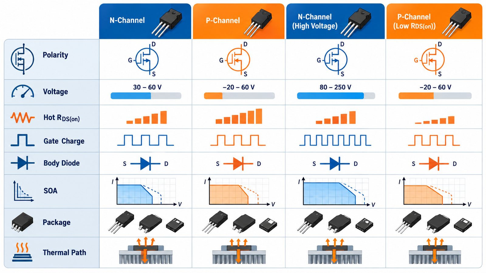
N-channel and P-channel devices require opposite gate polarity and have opposite body-diode orientation. Enhancement-mode devices are normally off at zero gate bias; depletion-mode devices are normally on. Replacing one with another changes startup and fault behavior even if voltage ratings match.
The introduction to what a MOSFET is covers these family distinctions.
Voltage and current ratings need context
Drain-source voltage needs margin for supply tolerance, ringing, inductive transients, and derating. Continuous-current numbers may be limited by an idealized case temperature, package leads, or PCB conditions. Pulsed current does not authorize indefinite operation, and avalanche ratings have defined test conditions.
Use current waveforms, SOA, and thermal impedance instead of choosing the largest number on the first page.
RDS(on) is not one fixed number
Resistance is specified at particular gate voltage and junction temperature. It rises with heat in ordinary silicon power MOSFETs and includes different contributions across voltage classes. A logic-level device is characterized for lower gate drive; a standard device may need about 10 V to reach its advertised resistance.
Package and PCB resistance can dominate ultra-low-resistance devices.
Dynamic parameters create tradeoffs
Gate charge, Miller charge, input and reverse-transfer capacitance, output capacitance, reverse-recovery charge, internal gate resistance, and package inductance affect switching. A larger die can reduce RDS(on) yet increase charge and capacitance, making the driver work harder and raising switching loss.
Selection for a buck converter is explored in choosing a buck-converter MOSFET.
Structure and technology matter
Planar, trench, superjunction, lateral, silicon-on-insulator, SiC, and other structures target different voltage and performance regions. Some devices prioritize low switching loss, some avalanche robustness, some linear operation, and some low leakage. Automotive-qualified parts add process and documentation requirements but are not automatically superior for every circuit.
Compare characterized behavior under the intended operating conditions.
Package and thermal path can decide the design
Through-hole, leaded surface-mount, bottom-cooled, top-cooled, chip-scale, and module packages transfer heat and current differently. The metal tab may be electrically live. Pin order, Kelvin-source options, creepage, mounting pressure, solder profile, and PCB copper requirements vary.
Use PCB thermal-path guidance before assuming equal package outlines mean equal cooling.
Turn the answer into a robust MOSFET design
For Are All MOSFETs the Same?, create an operating-state table before choosing a device or protection value. Include off, startup, steady on, PWM transitions, shutdown, reverse current, load connection, controller reset, brownout, open load, overload, and short circuit. For each state, write the expected VGS, VDS, current, duration, repetition, and starting temperature. This exposes short but severe events that an average-current calculation hides.
Next, compare the table with guaranteed data-sheet limits and characterized curves. Use voltage margin for supply tolerance and ringing; use RDS(on) at the actual gate voltage and hot junction; use total gate charge and Miller charge for driver sizing; and use DC or pulsed SOA for intervals where voltage and current coexist. Include package, PCB copper, interface material, airflow, connector, and source-return inductance in the model. A transistor cannot be evaluated separately from its commutation path and gate loop.
Build a staged test plan that begins with limited available energy. Capture gate-to-source voltage at the pins, drain-source voltage, current, and temperature while changing one stress at a time. Repeat enough cycles to reveal cumulative heating and recovery behavior. Define pass limits before looking at the waveform, preserve oscilloscope files, and record device lot, ambient, probe method, and firmware revision. If measured peaks approach an absolute maximum, redesign for margin rather than accepting the result because one prototype survived.
Practical validation checklist
Validate at the worst credible supply voltage, load current, switching frequency, ambient temperature, and fault condition. Measure gate-to-source voltage at the device pins, drain-to-source voltage with adequate bandwidth, current, case temperature, and—when power or pulses are significant—estimated junction temperature. Account for probe ground inductance and avoid interpreting ringing created by the measurement setup as circuit behavior.
Compare every result with the data-sheet safe operating area, absolute maximum ratings, transient thermal impedance, and temperature-dependent curves. Test startup, shutdown, load connection, stalled or shorted load, controller brownout, and repeated operation. The guides to reading MOSFET safe operating area and MOSFET thermal calculation provide useful companion checks.
Frequently asked questions
Can I substitute any MOSFET with the same voltage rating?
No. Current, hot resistance, gate drive, charge, SOA, diode behavior, package, pinout, and thermal performance must also fit.
Are logic-level MOSFETs always better?
No. They suit lower gate voltage, but other dynamic, leakage, ruggedness, cost, and availability tradeoffs remain.
Does a bigger MOSFET carry more current?
Not necessarily. Die, package, cooling, PCB, current waveform, and junction limits determine usable current.
Are SiC MOSFETs interchangeable with silicon MOSFETs?
No. They may require different gate drive, layout, protection, dead time, insulation, and EMI control.