To protect a MOSFET switching an inductive load, provide a controlled path for current when the MOSFET turns off. A motor winding, relay, solenoid, transformer leakage inductance, or even long wiring stores magnetic energy. Because current cannot change instantly, an interrupted path drives the drain voltage upward until something conducts.
The protective network must keep VDS below a safe level, absorb the stored energy at the required repetition rate, and produce acceptable release time. Layout inductance between the MOSFET and clamp also matters.
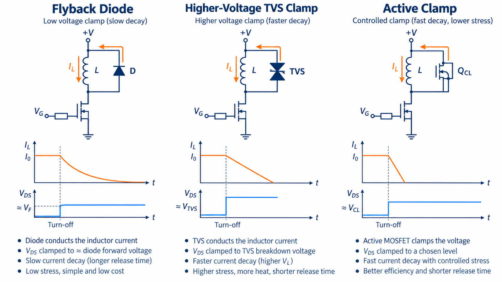
Estimate the stored energy
A first estimate is E = ½LI² at the moment of turn-off. Real loads have nonlinear inductance, resistance, moving parts, mutual coupling, and supply interaction, so measure current and decay as well. Repetitive energy per second contributes average heat, while one abnormal pulse may set avalanche or surge requirements.
Include cable inductance and the current that exists during stall, cold resistance, overvoltage, or control fault—not only nominal current.
Use a flyback diode for a slow low-voltage clamp
Across a DC coil, place the diode so it is reverse biased while energized and forward biased after turn-off. The low clamp voltage minimizes MOSFET stress but allows current to decay slowly, which can delay relay release or solenoid motion. Size the diode for initial current, pulse duration, repetition, hot leakage, and junction temperature.
The orientation examples in connecting a Schottky diode help prevent the common mistake of shorting the supply.
Use a higher clamp for faster release
A TVS, Zener-plus-diode, RCD network, or active clamp permits a higher voltage and therefore a faster current fall. Select a clamp level that remains below the MOSFET rating after tolerance, temperature, wiring overshoot, and supply variation. Ensure the load insulation and nearby electronics tolerate that voltage.
High clamp power can be brief but severe. Pulse rating must be evaluated at the waveform duration and repetition, not inferred from a headline wattage.
Treat avalanche as a designed operating condition
An avalanche-rated MOSFET may absorb energy after VDS reaches breakdown, but the data-sheet rating comes with current, starting temperature, pulse-shape, and test-circuit assumptions. Repetition can raise junction temperature and contribute to aging. Current crowding and unclamped inductive switching may be less forgiving in parallel devices.
Review single-pulse and repetitive avalanche before intentionally relying on the transistor.
Fix the physical current loop
Place the recirculation or clamp component close to the MOSFET and load connector so the high-di/dt loop is compact. A remote diode may clamp the load yet leave local trace and cable inductance to create a sharp drain spike. Use a close ceramic or film bypass path where the topology requires it and route gate and source returns away from the power loop.
Probe directly at drain and source with a low-inductance technique to see the true overshoot.
Coordinate faults and functional behavior
Test open load, shorted load, disconnected clamp, stalled actuator, repeated command, hot ambient, and controller reset. A freewheel diode can keep a safety-critical actuator energized longer than intended; a high-voltage clamp can release faster but increase EMI and insulation stress. Mechanical requirements therefore belong in the electrical protection decision.
Use the broader MOSFET protection framework for gate, overcurrent, and thermal layers around the inductive clamp.
Turn the answer into a robust MOSFET design
For How to Protect a MOSFET When Switching Inductive Loads, create an operating-state table before choosing a device or protection value. Include off, startup, steady on, PWM transitions, shutdown, reverse current, load connection, controller reset, brownout, open load, overload, and short circuit. For each state, write the expected VGS, VDS, current, duration, repetition, and starting temperature. This exposes short but severe events that an average-current calculation hides.
Next, compare the table with guaranteed data-sheet limits and characterized curves. Use voltage margin for supply tolerance and ringing; use RDS(on) at the actual gate voltage and hot junction; use total gate charge and Miller charge for driver sizing; and use DC or pulsed SOA for intervals where voltage and current coexist. Include package, PCB copper, interface material, airflow, connector, and source-return inductance in the model. A transistor cannot be evaluated separately from its commutation path and gate loop.
Build a staged test plan that begins with limited available energy. Capture gate-to-source voltage at the pins, drain-source voltage, current, and temperature while changing one stress at a time. Repeat enough cycles to reveal cumulative heating and recovery behavior. Define pass limits before looking at the waveform, preserve oscilloscope files, and record device lot, ambient, probe method, and firmware revision. If measured peaks approach an absolute maximum, redesign for margin rather than accepting the result because one prototype survived.
Practical validation checklist
Validate at the worst credible supply voltage, load current, switching frequency, ambient temperature, and fault condition. Measure gate-to-source voltage at the device pins, drain-to-source voltage with adequate bandwidth, current, case temperature, and—when power or pulses are significant—estimated junction temperature. Account for probe ground inductance and avoid interpreting ringing created by the measurement setup as circuit behavior.
Compare every result with the data-sheet safe operating area, absolute maximum ratings, transient thermal impedance, and temperature-dependent curves. Test startup, shutdown, load connection, stalled or shorted load, controller brownout, and repeated operation. The guides to reading MOSFET safe operating area and MOSFET thermal calculation provide useful companion checks.
Frequently asked questions
Do all inductive loads need a flyback diode?
They need a controlled energy path, but that path may be a diode, TVS, snubber, active clamp, regenerative bridge, or another topology.
Why did the MOSFET fail even with a diode?
The diode may be remote, slow, undersized, reversed, disconnected, or unable to clamp parasitic inductance near the switch.
Is a higher clamp voltage better?
It speeds current decay but raises MOSFET, insulation, EMI, and clamp-energy stress; choose it from system requirements.
Can the MOSFET body diode protect the drain?
Usually not in a simple low-side inductive switch because its orientation does not provide the required local turn-off path.