Yes, MOSFETs can switch AC, but a single ordinary power MOSFET is not a complete bidirectional off switch. Its enhanced channel can conduct current in either direction, while its intrinsic body diode conducts one polarity even when the gate is off. To block both halves of an AC waveform, designers commonly use two MOSFETs back to back or a bridge rectifier around one MOSFET.
For mains AC, isolation, creepage, clearance, overcurrent protection, surge rating, enclosure, and legal compliance are essential. Use certified solid-state relays or qualified design rather than exposed prototypes.
Why one MOSFET cannot turn AC fully off
With the channel off, the body diode remains. During one polarity it is reverse biased, but during the other it becomes forward biased. The load can therefore receive half-wave current. Reversing the MOSFET only reverses which half-cycle passes.
Bidirectional MOSFET conduction explains the distinction between on-state conduction and off-state blocking.
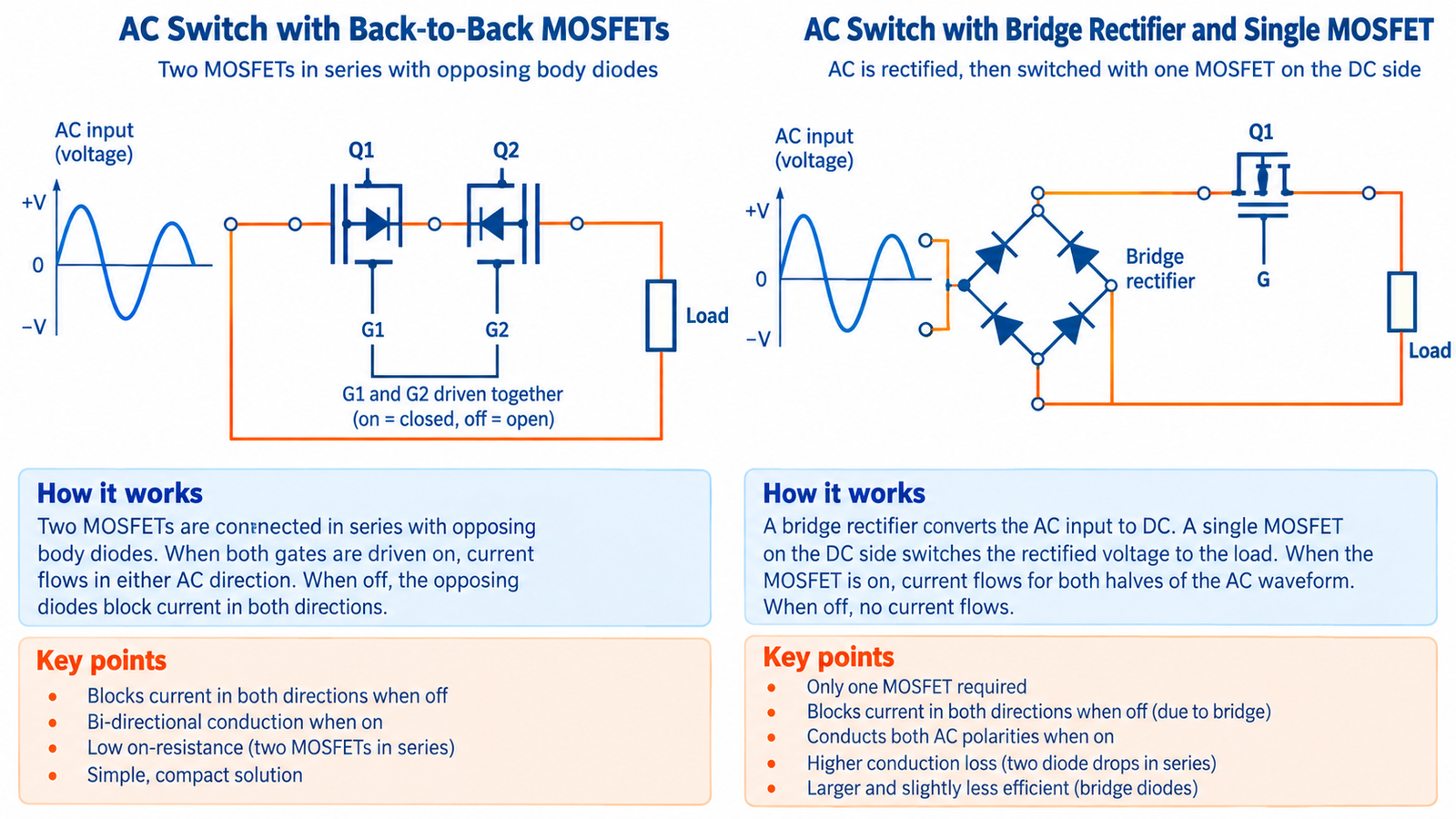
Use a back-to-back pair
Connect two N-channel MOSFETs in series so their body diodes oppose. Common-source and common-drain arrangements are both possible. When off, one diode blocks each polarity. When both channels are enhanced, AC current flows through two channel resistances. The gate drive must establish the required VGS relative to the moving source node.
Account for twice the hot on-resistance plus wiring and package loss.
Use a bridge plus one MOSFET
A diode bridge can steer either AC polarity through one MOSFET in the same direction. This simplifies gate reference but adds two diode drops in series with the load, creating loss and heat. The bridge and MOSFET must withstand peak AC voltage, surge current, and load transients.
At low voltage, those diode losses can outweigh the convenience.
Choose an appropriate gate drive
An isolated driver, photovoltaic optocoupler, isolated bias supply, or specialized AC-switch controller may be used. Verify turn-on time, turn-off current, maximum VGS, dV/dt immunity, isolation rating, and behavior when control power disappears. A simple ground-referenced microcontroller signal is not suitable for a source node that follows mains.
Gate protection should follow MOSFET gate-protection practice.
Consider switching timing and load type
Zero-cross turn-on can reduce inrush for some resistive loads, while phase control or arbitrary switching changes EMI and stress. Transformers, motors, capacitors, and inductors can create large inrush or turn-off voltage. A MOSFET pair does not inherently provide the same latching and commutation behavior as a triac.
Specify whether the load needs fast PWM, infrequent on/off control, or line-frequency phase control.
Design for mains safety and faults
Use components rated for peak line voltage plus surges, not RMS voltage alone. Provide a fuse, MOV or surge network as required, thermal protection, flame-rated enclosure, and PCB spacing appropriate to working voltage and pollution degree. Analyze a MOSFET failed short, driver failed on, open neutral, and loss of control power.
For mains products, certification and qualified review are part of the design, not optional paperwork.
Turn the answer into a robust MOSFET design
For Can a MOSFET Switch AC?, create an operating-state table before choosing a device or protection value. Include off, startup, steady on, PWM transitions, shutdown, reverse current, load connection, controller reset, brownout, open load, overload, and short circuit. For each state, write the expected VGS, VDS, current, duration, repetition, and starting temperature. This exposes short but severe events that an average-current calculation hides.
Next, compare the table with guaranteed data-sheet limits and characterized curves. Use voltage margin for supply tolerance and ringing; use RDS(on) at the actual gate voltage and hot junction; use total gate charge and Miller charge for driver sizing; and use DC or pulsed SOA for intervals where voltage and current coexist. Include package, PCB copper, interface material, airflow, connector, and source-return inductance in the model. A transistor cannot be evaluated separately from its commutation path and gate loop.
Build a staged test plan that begins with limited available energy. Capture gate-to-source voltage at the pins, drain-source voltage, current, and temperature while changing one stress at a time. Repeat enough cycles to reveal cumulative heating and recovery behavior. Define pass limits before looking at the waveform, preserve oscilloscope files, and record device lot, ambient, probe method, and firmware revision. If measured peaks approach an absolute maximum, redesign for margin rather than accepting the result because one prototype survived.
Practical validation checklist
Validate at the worst credible supply voltage, load current, switching frequency, ambient temperature, and fault condition. Measure gate-to-source voltage at the device pins, drain-to-source voltage with adequate bandwidth, current, case temperature, and—when power or pulses are significant—estimated junction temperature. Account for probe ground inductance and avoid interpreting ringing created by the measurement setup as circuit behavior.
Compare every result with the data-sheet safe operating area, absolute maximum ratings, transient thermal impedance, and temperature-dependent curves. Test startup, shutdown, load connection, stalled or shorted load, controller brownout, and repeated operation. The guides to reading MOSFET safe operating area and MOSFET thermal calculation provide useful companion checks.
Frequently asked questions
Can one MOSFET switch 12 VAC?
It can control the channel, but its body diode passes one polarity when off; use a bidirectional arrangement if full isolation is required.
Why use two MOSFETs source to source?
Their body diodes oppose, so the off pair blocks both current directions while a shared gate reference can drive both channels.
Is a MOSFET AC switch better than a triac?
It can offer low-voltage-drop and DC turn-off advantages, but drive, surge, cost, and mains safety differ by application.
Can I PWM mains AC with MOSFETs?
Specialized converters can, but high-voltage switching, EMI, isolation, protection, and compliance require professional design.