Read a power MOSFET datasheet by matching each number to its test conditions and the intended circuit. Start with the package and absolute limits, then check guaranteed on-resistance at your gate voltage, gate charge at relevant drain bias, and safe operating area for the real pulse. Finish with thermal data and measured margins on the assembled board.
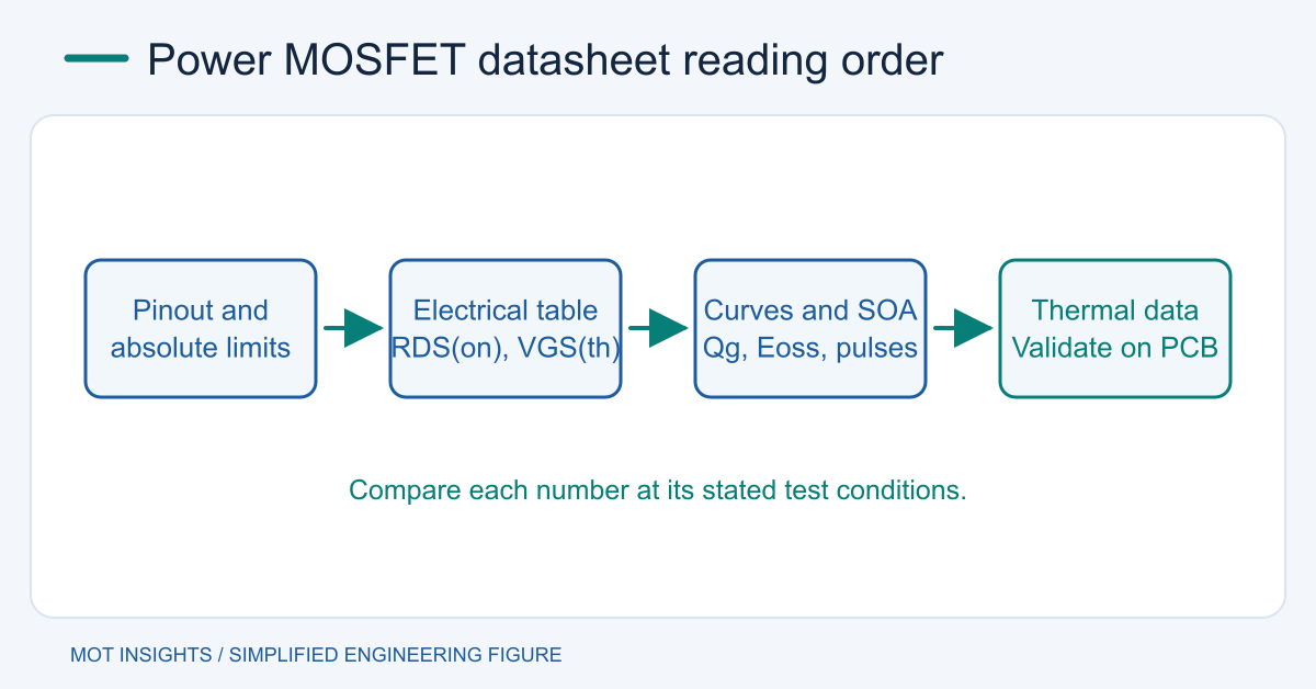
Start with the package drawing
Check device polarity, pin numbering and the view direction of the drawing. Confirm the exposed pad and whether a Kelvin source is provided. Two packages with similar outlines can differ in land pattern, gate location and current path. Verify the exact ordering code and package revision, especially for a substitute.
Read maximum ratings as constraints
VDS, VGS and junction-temperature limits establish stress boundaries. Allow for line and load transients, overshoot and temperature. Continuous ID may assume a controlled case temperature and may be limited by the package. Your board and cooling determine usable current. A pulsed current rating also has duration, temperature and duty conditions. Use the MOSFET selection guide to map circuit conditions to the limits.
Find the guaranteed values in the electrical table
Read maximum RDS(on) at the lowest usable gate voltage that the data sheet explicitly covers. Check the drain-current and temperature conditions. VGS(th) is measured at a small drain current and establishes conduction onset under a specific test. A logic output that merely exceeds threshold can still leave high channel resistance. Review threshold extraction and test conditions when comparing devices with different threshold definitions.
For example, if maximum room-temperature RDS(on) is 8 mΩ at the intended drive, and a validated design estimate uses 1.6 times that value hot, 10 A RMS yields about 1.28 W of channel conduction loss. If the multiplier comes from a typical curve, it is a design estimate. Check hot limits, sample variation and actual gate voltage before relying on it.
Read curves at the right operating point
Use gate charge curves to size the driver. Check VDS, ID and final gate voltage used in the graph. Qgd describes the Miller interval, and total Qg helps estimate average driver power. Switching time values depend on the manufacturer’s driver, gate resistor and test circuit. Compare nonlinear Coss curves or Eoss at the intended drain voltage. Examine diode forward drop and reverse recovery if the device commutates reverse current.
The transfer curve is typically an illustrative device response, while the guaranteed table defines tested limits. For linear operation, check the SOA graph at the applied voltage, current and pulse duration. Read its case-temperature assumption, and examine whether your pulse repeats. Use the MOSFET SOA guide for the limitations of pulse scaling.
Close the thermal calculation on the real board
Use a thermal resistance appropriate to the path and its reference temperature. RθJC depends on where the case temperature is defined. RθJA reflects the specified board and ambient conditions. For a short power pulse use transient thermal impedance with the proper boundary and repetition. Estimate switching, channel and diode losses separately before adding them. Validate with case or board measurements and a credible junction-temperature estimate.
Record a selection table with each parameter, test condition, design requirement and margin. Compare MOT power MOSFETs on common electrical and thermal conditions before choosing a footprint or substitute.