A vertical insulated-gate AlGaN/GaN heterojunction field-effect transistor routes electrons laterally in a high-mobility heterojunction channel and then vertically through current apertures into a GaN drift region and backside drain. This hybrid geometry was demonstrated on a free-standing GaN substrate as an early prototype for high-power vertical GaN switching.
The title refers to work reported by Masakazu Kanechika and coauthors in the Japanese Journal of Applied Physics in 2007 and later summarized by Toyota Central R&D Labs. The prototype is important historically because it joined AlGaN/GaN two-dimensional electron gas conduction with a vertical current path. It should not be confused with every modern vertical GaN MOSFET or current-aperture vertical electron transistor.
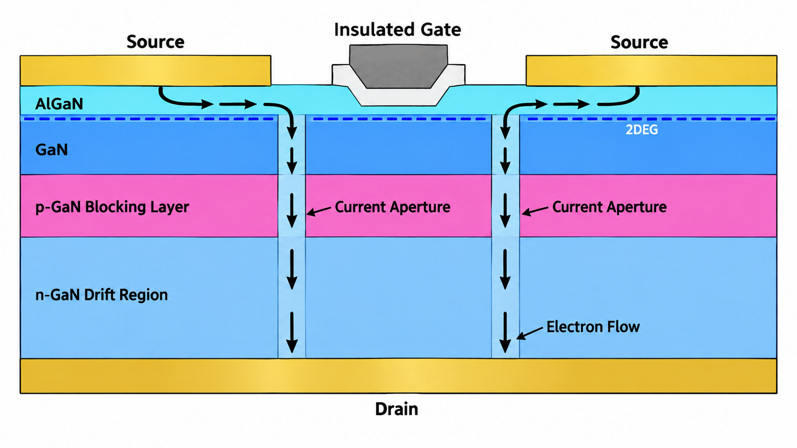
What the device structure contains
At the surface, an AlGaN barrier on GaN creates a high-density two-dimensional electron gas, commonly abbreviated 2DEG. Source contacts connect to this lateral channel. An insulated gate controls charge in the channel without relying on a direct Schottky gate contact. Beneath the surface is a p-GaN current-blocking layer with narrow openings.
The openings are current apertures. They were formed by etching the p-GaN and regrowing lightly doped n-type GaN. When the device conducts, electrons move from each source along the heterojunction channel, turn downward through an aperture, enter the n-GaN drift region, and leave through the drain on the back of the GaN substrate.
Why use a vertical geometry?
In a lateral HEMT, source, gate, and drain are placed on the top surface, and voltage is supported mainly across a lateral spacing. Increasing voltage normally requires a longer drift distance and consumes die area. In a vertical device, the voltage-supporting region extends through the wafer thickness. Current capability can scale with chip area while voltage capability can scale with drift-region thickness and doping.
A backside drain can also make high-current packaging more direct. However, the vertical approach requires high-quality native or free-standing GaN, controlled vertical doping, low-resistance backside contacts, uniform current apertures, and electric-field termination. These manufacturing challenges historically made lateral GaN-on-silicon devices easier to commercialize.
What “insulated gate” changes
An insulating layer separates the gate electrode from the semiconductor. In principle this reduces DC gate leakage and lets the gate electrostatically control the channel. In practice, interface traps, oxide charge, electric-field crowding, and dielectric reliability become critical. The gate dielectric must survive repeated switching and the electric field around the aperture without drifting in threshold or leaking.
The mechanism still resembles a field-effect switch. The broader explanation in how a MOSFET transistor works is useful for understanding voltage-controlled conduction, although an AlGaN/GaN HFET uses a heterojunction channel rather than a conventional silicon inversion channel.
Reported prototype performance
The 2007 paper reported a specific on-resistance as low as 2.6 mΩ·cm² and a threshold voltage near −16 V. Specific on-resistance normalizes resistance to active area so researchers can compare structures of different size. The result demonstrated that the regrown apertures and vertical drift path could conduct with low resistance for an early device.
The strongly negative threshold means the prototype was normally on: at zero gate-to-source voltage it conducted. That behavior is undesirable for most fail-safe power converters, which prefer a normally-off switch. Later vertical GaN research has therefore explored p-GaN gates, trench MOS structures, aperture engineering, and other approaches to achieve enhancement-mode operation.
How the current-blocking layer works
The p-GaN layer prevents current from flowing everywhere beneath the surface. Current is funneled through selected n-GaN apertures. The gate and heterojunction channel regulate how much electron current reaches those openings. Aperture width, spacing, doping, regrowth interface quality, and alignment affect resistance and current distribution.
If apertures are too narrow, current crowding and resistance increase. If they are too wide or poorly controlled, off-state leakage and electric-field stress may rise. Local defects at the etched and regrown interface can act as traps or leakage paths. Uniform processing across the die is therefore as important as the ideal cross-section.
Electric-field and breakdown challenges
The drift region must support the off-state voltage without avalanche or excessive leakage. Field crowding can occur near the gate edge, aperture corners, p-n junctions, and die perimeter. Designers use field plates, guard structures, edge termination, optimized doping, and careful dielectric geometry to spread the field.
GaN’s wide bandgap and high critical electric field make the material attractive, but real breakdown depends on defects, surface states, buffer quality, and edge design. A material property does not automatically become a device rating. As with high-voltage wide-bandgap gate-drive design, the complete electric-field and switching environment must be validated.
Dynamic performance and trapping
Heterojunction devices can show current collapse or dynamic on-resistance when trapped charge changes the channel after high-voltage stress. Vertical structures add regrowth interfaces and buried junctions that may introduce more trap locations. Static on-resistance therefore does not fully describe switching performance.
Useful characterization includes pulsed I-V measurements, dynamic RDS(on), capacitance versus voltage, gate charge, switching loss, leakage, threshold stability, and breakdown after repeated stress. A low-inductance test fixture is essential because fast GaN transitions can make fixture overshoot look like device behavior. The principles in gate-resistor and EMI tuning remain relevant during evaluation.
How this prototype relates to modern vertical GaN
The early device proved a path rather than defining one commercial standard. Modern vertical GaN research includes current-aperture vertical electron transistors, vertical trench FETs, fin-channel devices, junction field-effect structures, and vertical diodes. Some retain an AlGaN/GaN 2DEG near the surface; others use MOS-controlled bulk or fin channels.
The common objective is to combine high breakdown voltage, low specific on-resistance, normally-off operation, low gate charge, manufacturable wafers, stable dielectrics, and robust short-circuit or avalanche behavior. Packaging and thermal extraction are also decisive, as discussed in power-device thermal-path design.
Questions engineers should ask
- Is the device normally off at all specified temperatures and bias histories?
- What voltage does the active area and edge termination actually sustain?
- How much does on-resistance increase after high-voltage off-state stress?
- How uniform are aperture resistance and current density across the die?
- What dielectric and interface lifetime has been demonstrated?
- How is the backside drain attached and cooled in a low-inductance package?
- What happens during short circuit, surge, and unclamped inductive switching?
Frequently asked questions
Is this device a conventional MOSFET?
No. It is an insulated-gate heterojunction FET that uses an AlGaN/GaN 2DEG and vertical current apertures. It shares voltage-controlled behavior with a MOSFET but has a different channel and structure.
Was the reported prototype normally off?
No. A threshold near −16 V indicates normally-on operation. Normally-off behavior is a major requirement for most practical power switches.
Why use a free-standing GaN substrate?
It enables a high-quality vertical GaN drift path and a backside drain without forcing current through a foreign substrate such as silicon or sapphire.