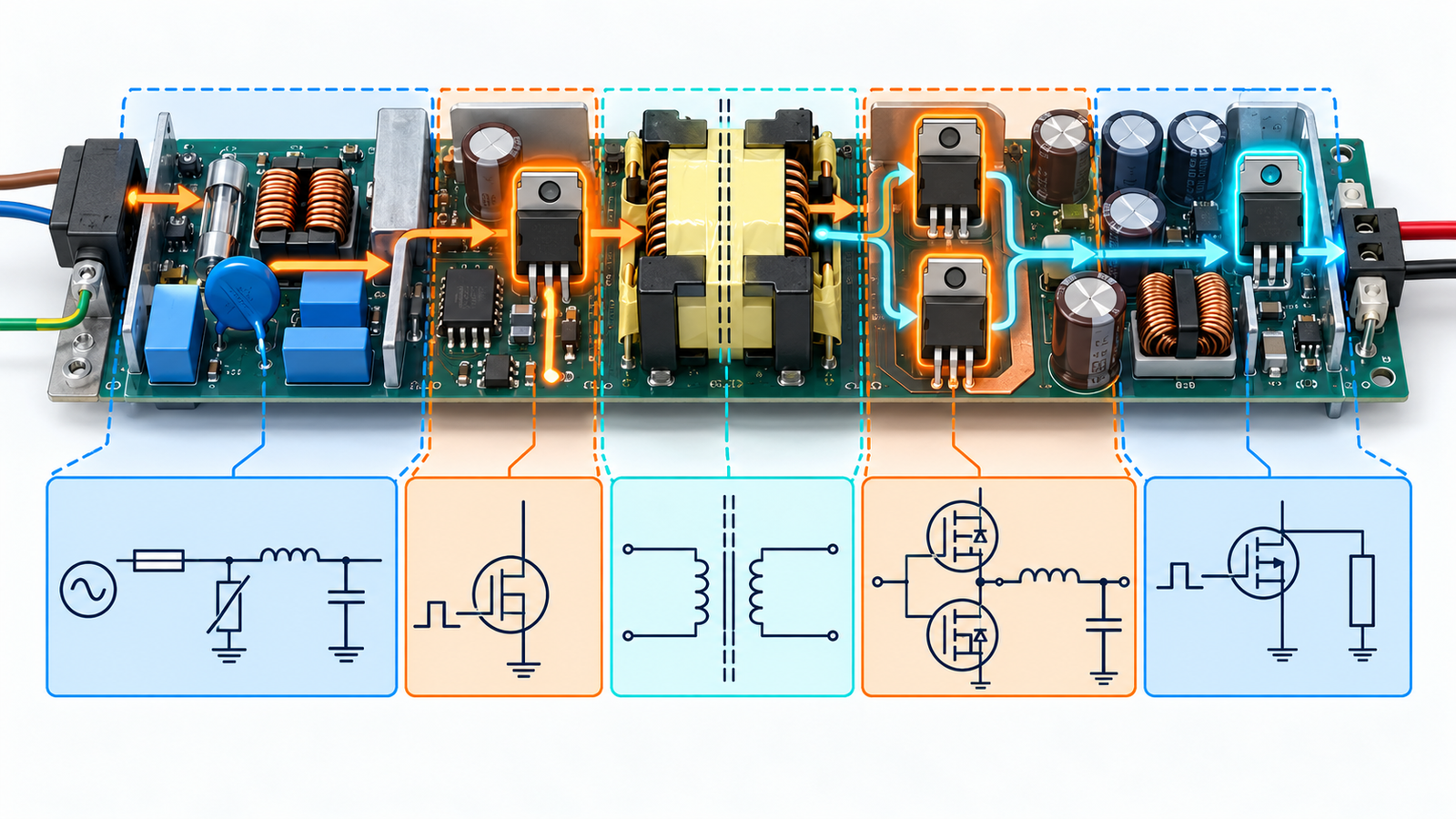
A MOSFET power supply is usually a switching power supply that uses one or more MOSFETs to control the flow of energy. The term is informal rather than a distinct converter category. A MOSFET may chop a DC bus into a transformer, switch current through an inductor, replace a diode for synchronous rectification, disconnect a faulted load, or provide reverse-polarity protection.
The MOSFET is important, but it is only one part of the converter. The controller, gate driver, magnetics, rectifiers, capacitors, feedback loop, PCB layout, cooling, and protection determine whether the complete supply is efficient and reliable.
Why power supplies use MOSFETs
A MOSFET is voltage controlled and can move between off and low-resistance states quickly. When fully enhanced, its drain-to-source resistance can be low; while transitioning, its capacitances and gate charge determine how much energy the driver must move. These traits make MOSFETs practical from low-voltage buck converters to offline flyback, forward, half-bridge, full-bridge, and resonant supplies.
The primer on how a MOSFET transistor works explains the gate, channel, and body diode that underlie these power-supply roles.
Primary-side switching
In an offline converter, the primary MOSFET repeatedly connects a rectified high-voltage bus to a transformer or inductor. It must block the bus plus leakage-inductance overshoot when off and carry peak current when on. The controller sets its timing, while the driver must charge and discharge the gate fast enough to limit transition loss without creating excessive ringing or EMI.
A clamp or snubber manages leakage energy. Current sensing and cycle-by-cycle limiting help protect the device, but turn-off delay, transformer saturation, poor layout, or an incorrectly chosen voltage margin can still destroy it.
Synchronous rectification
At low output voltage, a diode’s forward drop can consume a large fraction of delivered power. A synchronous rectifier uses a MOSFET as an actively timed low-resistance path. This can improve efficiency in server, telecom, computing, battery, and USB power systems. Timing is critical: turning on at the wrong moment can create reverse current or a shoot-through path.
The MOSFET body diode may conduct briefly during dead time, but it is not always an efficient continuous rectifier. The controller, gate loop, current direction, and package inductance must support clean commutation.
Protection and power-path MOSFETs
MOSFETs are also used as electronic fuses, hot-swap switches, battery disconnects, ideal-diode elements, and reverse-polarity protectors. In these jobs the device may spend time in its linear region while charging a capacitor or limiting current. A low RDS(on) alone is not enough; the data-sheet safe-operating-area graph must support the voltage, current, duration, and case temperature.
Back-to-back MOSFETs can block current in both directions because one intrinsic body diode alone would otherwise conduct. Gate-source clamps and controlled slew rate protect the oxide and limit inrush.
How to choose the MOSFET
Start with repetitive and transient drain voltage, RMS and peak current, switching frequency, topology, junction-temperature target, and available gate voltage. Use hot RDS(on), not only the 25 °C figure. Estimate turn-on, turn-off, output-capacitance, reverse-recovery, conduction, and gate-drive losses. Check package thermal resistance and the actual heat path to copper or heatsink.
The selection workflow in choosing a MOSFET for a buck converter shows how competing specifications change between high-side and low-side positions.
Why MOSFETs fail in power supplies
Common causes include avalanche from leakage inductance, excessive VDS, gate-oxide spikes, cross-conduction, transformer saturation, insufficient dead time, driver undervoltage, overheating, poor soldering, and output faults. Fast switching also makes parasitic inductance visible. A device can fail short and damage the fuse, rectifier, gate driver, current-sense network, or load.
When a supply fails, do not replace the MOSFET and immediately apply full mains. The safer process in repairing a switch-mode power supply emphasizes isolation, discharge, current limiting, causal diagnosis, and post-repair validation.
Practical design review
Map every MOSFET to its function and switching state. Record the maximum off-state voltage, current waveform, gate voltage, frequency, dead time, thermal path, and expected fault energy. Review the high-di/dt commutation loop and high-dV/dt switch node on the PCB. Keep the driver close, provide a low-inductance source return, place decoupling at the driver, and avoid routing control traces under noisy copper.
Prototype with safe energy limits and measure VDS, VGS, current, and temperature using probes suited to the common-mode voltage and bandwidth. Test startup, shutdown, pulse skipping, overload, short circuit, minimum and maximum input, and hot operation. If the device is hot, separate conduction and switching loss before enlarging the heatsink; whether switching reduces MOSFET heat depends on the waveform and operating point.
For production, lock the exact device suffix, approved alternatives, gate resistor values, driver supply limits, snubber parts, and thermal assembly. Audit substitutions against measured switching energy and waveforms, not only voltage and current ratings. Record oscilloscope setup and probe location so later troubleshooting reproduces the same conditions.
Frequently asked questions
Does every switching power supply use a MOSFET?
No. Some use BJTs, IGBTs, GaN transistors, integrated power stages, or combinations. MOSFETs are extremely common across low- and medium-power converters.
Is a power MOSFET the same as a power supply?
No. The MOSFET is a semiconductor component inside a circuit; the power supply is the complete energy-conversion system.
Can I replace a failed supply MOSFET with any part of the same voltage?
No. Current, hot resistance, gate charge, switching energy, body-diode behavior, avalanche rating, package, pinout, and driver compatibility also matter.
Why are several MOSFETs connected in parallel?
Parallel devices can reduce conduction loss and distribute heat, but their gate and current paths must be symmetrical and their dynamic sharing verified.