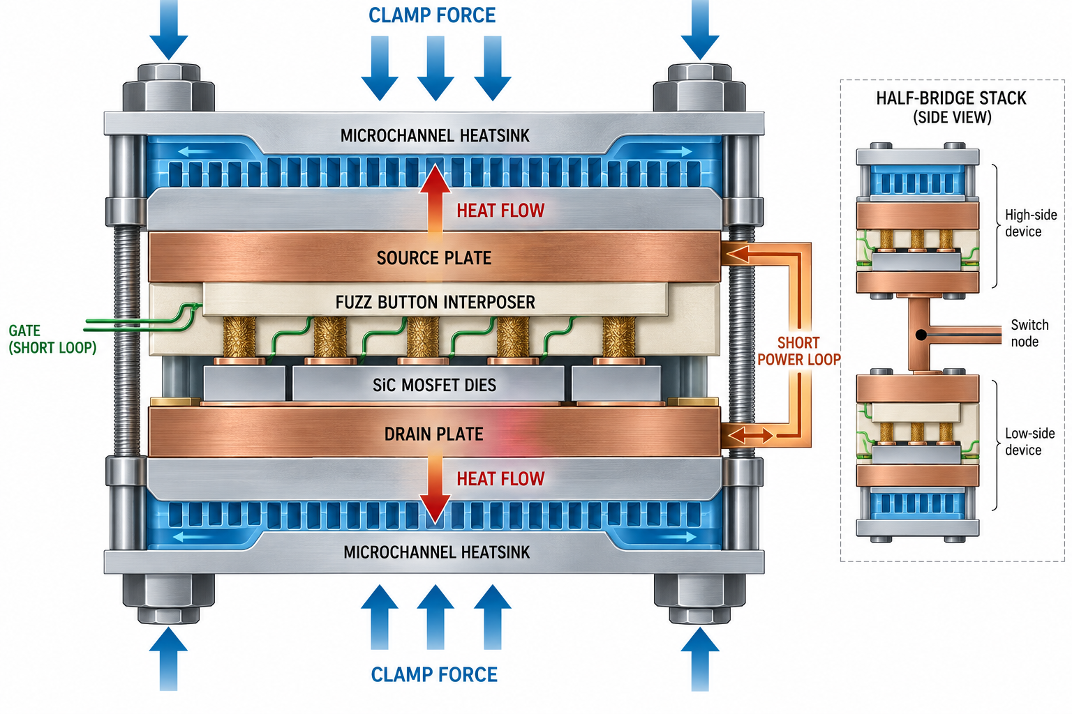
A practical press-pack packaging solution for SiC MOSFETs uses miniature flexible pressure contacts, called fuzz buttons, inside a low-profile interposer to connect the top of multiple bare dies. Thin microchannel heatsinks are integrated into the clamped electrical stack to remove heat from both sides without creating an excessively large power-loop inductance.
This architecture was presented by Nan Zhu and coauthors in the 2017 IEEE Transactions on Industrial Electronics paper “A Solution to Press-Pack Packaging of SiC MOSFETs,” DOI 10.1109/TIE.2017.2686365. The work addresses the mismatch between traditional press-pack construction and the small, fast-switching, mechanically sensitive structure of SiC MOSFET dies. It demonstrates feasibility through a press-pack design and a half-bridge stack evaluated by simulation and experiment.
What is press-pack packaging?
A press-pack power semiconductor is held between conductive electrodes by an external clamping system. Mechanical pressure maintains the electrical and thermal interfaces. Traditional high-power press-pack devices are valued for double-sided cooling, low-inductance bus structures, modular series stacking, and failure behavior that can be useful in some grid applications.
Press-pack is not the same as press-fit. Press-fit usually describes compliant terminal pins inserted into plated PCB holes. Press-pack describes a semiconductor assembly whose main current and heat paths depend on controlled compression across the device stack.
Why conventional SiC packaging becomes a limitation
SiC MOSFETs can switch rapidly and operate at high electric field and heat flux. A conventional module with wire bonds, a soldered die attach, and single-sided cooling introduces parasitic inductance, thermal interfaces, and fatigue-prone joints. Faster current edges convert a small inductance into significant voltage overshoot, while concentrated loss makes the thermal path increasingly important.
Packaging therefore becomes part of the electrical design. Gate-loop inductance, common-source inductance, power-loop symmetry, current sharing, and heat spreading can determine whether the system realizes the device’s datasheet performance. The article on power MOSFET thermal paths explains the same junction-to-coolant principle at board scale.
Why SiC MOSFETs are difficult to press-pack
Small and brittle dies
SiC dies are comparatively small for their power rating and mechanically brittle. A rigid point contact or uneven clamping force can create local stress, crack the die, or damage top-side metallization. The contact system must accommodate thickness and flatness tolerances while distributing force.
Separate source and gate connections
A MOSFET needs a high-current source connection and a low-inductance gate-return path. A simple large-area pressure electrode cannot blindly contact every top-side region. The package must route gate, Kelvin source, and power source separately without sacrificing insulation or pressure uniformity.
Fast-switching parasitics
SiC’s high dv/dt and di/dt make a physically long clamp, heatsink, or bus path electrically expensive. Common-source inductance couples power current into gate voltage and can slow switching, cause ringing, or unbalance parallel dies.
Insulation and cooling interaction
A press-pack does not automatically insulate the active semiconductor from its external cooling hardware. If a heatsink becomes part of the main electrical stack, its voltage potential, coolant isolation, creepage, clearance, and common-mode capacitance must be designed as power-circuit parameters.
The fuzz-button interposer solution
The proposed architecture places miniature elastic contacts in a low-profile ceramic interposer. Each fuzz button is a compressed bundle of fine conductive wire that can provide vertical electrical contact while accommodating small height differences. Arrays of contacts connect the source metallization of each die, while dedicated paths route the gate and its return.
Flexibility is the key mechanical advantage. Instead of concentrating the entire clamp load through one rigid pin, many compliant contacts share pressure and tolerate assembly variation. The interposer also fixes contact locations so gate and source regions are not confused during assembly.
The solution removes conventional top-side wire bonds. That can shorten current paths and avoid bond-wire lift-off as a dominant ageing mechanism, but it introduces new reliability questions: contact resistance drift, fretting, oxidation, loss of preload, particle contamination, and interposer deformation must be tested over the mission profile.
Low-profile microchannel heatsinks
The architecture uses thin microchannel heatsinks close to the active dies. Coolant flowing through many small channels provides a large heat-transfer area in a low profile. Cooling both sides reduces the distance from the junction to coolant and can lower temperature gradients across a parallel die array.
Low profile is electrically important. A thick conventional cold plate inside the commutation path would enlarge the half-bridge loop and add stray inductance. The proposed thin heatsink allows two press packs and three cooling layers to form a compact half-bridge stack.
Coolant plumbing must remain electrically isolated from the energized stack. Dielectric strength, corrosion, conductivity change, leak detection, pressure drop, pump reliability, and galvanic compatibility are part of the package qualification, not secondary mechanical details.
Electrical loop and current sharing
Parallel SiC dies require closely matched drain, source, and gate impedances. A symmetric layout gives each die a similar power-loop inductance and resistance. Gate paths should also be matched so one die does not turn on earlier and carry excessive dynamic current.
Kelvin source routing separates gate-driver return current from the voltage developed by the main source current. Individual gate resistors can damp local oscillation, but their value and placement must be coordinated with the common driver. Guidance on negative gate bias for SiC MOSFETs shows how package inductance and gate voltage interact during fast switching.
Validate the module with double-pulse tests at the intended DC-link voltage, current, junction temperature, and gate resistance. Measure current sharing among dies, not only the terminal current. Overshoot, ringing, switching energy, common-mode current, and cross-talk should be correlated with an extracted parasitic model.
Mechanical pressure is a design variable
Too little clamp force increases contact resistance and creates local heating. Too much force can fracture SiC, deform the interposer, damage metallization, or overload the ceramic and heatsink. The clamping structure should apply a specified force across temperature, vibration, manufacturing tolerance, and long-term relaxation.
Finite-element mechanical analysis can predict pressure distribution, but measurements are still required. Pressure-sensitive film, load cells, dimensional inspection, contact-resistance mapping, and acoustic or X-ray inspection can reveal nonuniform assembly. The design should prevent a tolerance stack from placing the entire load on one die.
Thermal and electrical insulation co-design
Every added electrical insulator tends to add thermal resistance, and every conductive heat spreader can create an unwanted electrical path or capacitance. The stack must balance junction-to-coolant resistance, electric field stress, partial discharge, common-mode capacitance, and mechanical compliance.
At medium or high voltage, pay special attention to triple points where conductor, dielectric, and air or coolant boundaries meet. Rounded electrodes, controlled field grading, sufficient creepage, void-free ceramics, and verified coolant isolation reduce localized field enhancement.
Half-bridge integration
The paper’s demonstrator stacks a high-side press pack and a low-side press pack with three microchannel heatsinks. This arrangement creates a compact phase leg with short connections between the devices and switch node. It also places cooling hardware at different electrical potentials, which changes how plumbing, sensors, gate drivers, and enclosure grounding must be arranged.
The driver should sit close to the gate interposer and provide controlled source and sink current. Protection must react within the short-circuit withstand time of the specific SiC device. Review the voltage and gate-drive context in 800 V SiC MOSFET gate-drive design.
Potential benefits
- Wire-bondless top contact: shorter paths and removal of bond wires as a fatigue mechanism.
- Double-sided cooling: lower thermal resistance and more uniform die temperature are possible.
- Compact commutation loop: a thin stacked structure can limit parasitic inductance.
- Modular high-power scaling: several parallel dies and stacked press packs can build larger switches and phase legs.
- Service-oriented clamping: a pressure-held assembly may support controlled disassembly during development, although a production design still needs stable force and sealing.
Limitations and qualification risks
- Pressure contacts can develop variable resistance through relaxation, oxidation, fretting, or contamination.
- SiC dies and ceramic layers remain sensitive to local mechanical stress.
- Liquid cooling adds seals, pumps, connectors, corrosion control, and leak-fault analysis.
- Heatsinks at switching potential complicate isolation, sensing, and common-mode EMI.
- Parallel dies require static and dynamic current-sharing verification.
- The architecture is a research-backed packaging approach, not a drop-in replacement for every commercial module.
Application value depends on the complete converter. The SiC upgrade path for EV traction illustrates how module, driver, cooling, busbar, and control changes must be considered together.
Recommended development workflow
- Define voltage, current, switching frequency, coolant, ambient, and lifetime mission profile.
- Select dies and determine the number of parallel chips from hot conduction and switching loss.
- Design source, gate, Kelvin source, and drain contact patterns around actual die metallization.
- Model clamp pressure, die stress, interposer compression, and thermal expansion.
- Co-simulate power-loop inductance, gate-loop inductance, electric field, common-mode capacitance, and thermal paths.
- Build coupon tests for fuzz-button resistance, preload relaxation, temperature cycling, vibration, humidity, and coolant exposure.
- Characterize a single press pack before assembling a half bridge.
- Run double-pulse, short-circuit, power-cycling, thermal-cycling, partial-discharge, and insulation tests.
- Define manufacturing controls for cleanliness, flatness, alignment, torque, clamp force, sealing, and traceability.
Frequently asked questions
Does press-pack mean the SiC die is squeezed directly between metal plates?
Not in a robust design. Compliant contacts, interposers, pressure spreaders, and controlled surfaces distribute force and route source and gate connections without damaging the die.
What is a fuzz button?
It is a miniature compliant electrical contact formed from densely packed fine wire. Under compression it provides a vertical conductive path and accommodates small dimensional differences.
Why use a microchannel heatsink?
Microchannels provide strong liquid heat transfer in a thin plate. The small thickness supports double-sided cooling while keeping the electrical commutation loop compact.
Is the heatsink electrically isolated from the MOSFET?
Not automatically. In this type of stack the cooling plate can be part of or closely coupled to the electrical path. Its potential, coolant isolation, capacitance, and external plumbing must be engineered deliberately.
Can press-pack packaging eliminate all SiC reliability problems?
No. It removes or changes some wire-bond and solder-related stresses but introduces pressure-contact, mechanical, sealing, insulation, and coolant reliability requirements. Qualification must match the intended mission profile.