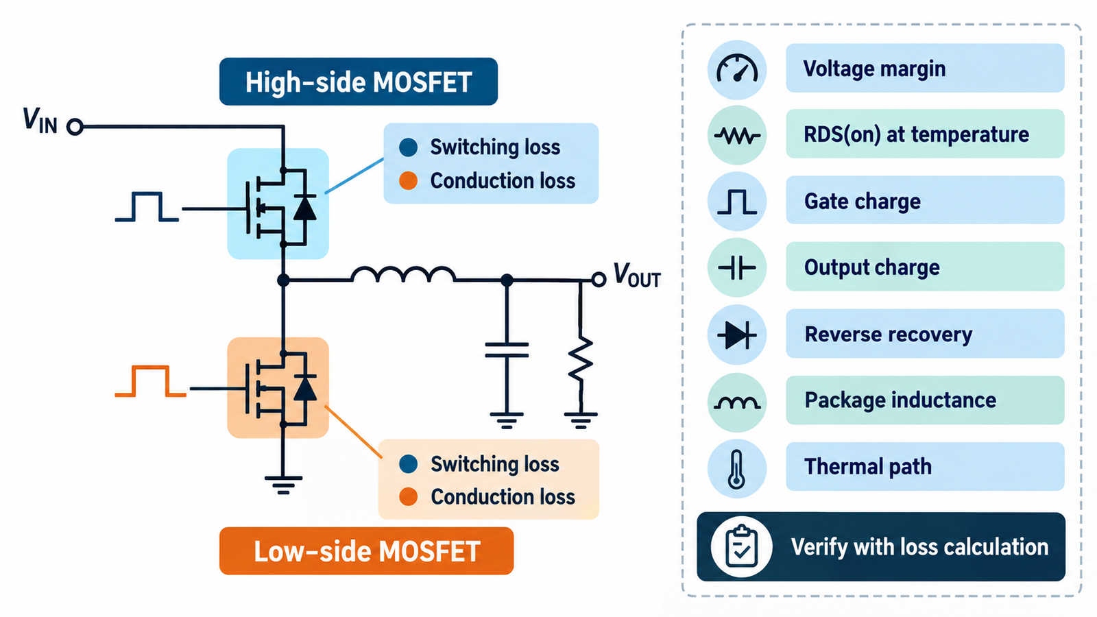
Select a buck-converter MOSFET by minimizing total system loss while meeting voltage, current, thermal, drive, layout, and fault requirements. Begin with maximum input voltage and transient overshoot, calculate high-side and low-side RMS currents, then compare conduction loss, switching loss, gate-drive loss, output-capacitance loss, reverse-recovery effects, and package thermal performance.
The high-side and synchronous low-side positions usually favor different tradeoffs. A very large, low-resistance MOSFET can reduce conduction loss yet increase charge, capacitance, switching loss, driver loss, cost, and layout area.
Define the buck operating range
Record minimum and maximum input, output voltage, continuous and peak load, switching frequency, ripple target, ambient, airflow, transient requirements, and fault strategy. Duty ratio is approximately VOUT/VIN for an ideal continuous-conduction buck, but dead time, losses, minimum on-time, and dropout alter the real value.
For the surrounding design process, use how to design a switch-mode power supply. MOSFET selection depends on inductor ripple, controller timing, driver voltage, and PCB geometry.
Choose drain-source voltage with margin
The high-side switch sees approximately the input voltage when off, plus ringing from the commutation loop. The low-side device sees a similar switch-node stress. Choose VDS rating above the worst input tolerance, surge, hot-plug event, and measured overshoot. More voltage rating can increase resistance and charge, so excessive margin has a cost.
Reduce overshoot with a tight input-capacitor loop, suitable package, controlled edge rate, and snubber when justified. Do not compensate for poor layout solely by selecting a much higher-voltage MOSFET.
Calculate conduction loss at temperature
Approximate MOSFET conduction loss with IRMS2RDS(on). The high-side conducts for duty D and the low-side for roughly 1 − D, excluding dead time. Include inductor ripple when calculating RMS current. Use the maximum RDS(on) at the available gate voltage and estimate its rise at operating junction temperature.
At low output voltage, the low-side device often carries current for most of the cycle, favoring low resistance. At a high duty ratio, high-side conduction matters more. Parallel devices may help but add gate charge and current-sharing complexity.
Estimate switching and capacitive losses
High-side turn-on and turn-off commonly dominate switching overlap because it commutates the switch node. Loss depends on input voltage, load current, transition time, frequency, gate charge, driver resistance, common-source inductance, and Miller behavior. Output capacitance stores energy each cycle, and nonlinear COSS data should be interpreted through energy or charge curves.
The low-side device contributes dead-time conduction and reverse-recovery or reverse-charge effects that can increase high-side turn-on stress. The article on whether switching a MOSFET reduces heat explains why switching operation is efficient but not lossless.
Match the gate driver
Confirm the controller’s gate-drive voltage fully enhances the selected MOSFET. Logic-level labeling alone is insufficient; check RDS(on) at the actual voltage. Total gate charge determines peak driver current and average drive power. A weak driver lengthens transitions, while an excessively fast driver can worsen overshoot, EMI, and false turn-on.
Use separate turn-on and turn-off resistances when needed. Apply the measurement method in tuning the gate resistor to balance efficiency, ringing, and emissions.
Check package, thermal path, and layout
Package resistance and inductance affect both heat and switching. Leadless packages can provide low loop inductance and strong PCB heat spreading but require good land patterns, copper, vias, and assembly. Calculate junction temperature from individual losses and the appropriate transient or steady-state thermal model. Account for the other MOSFET and inductor heating the same board region.
Use the PCB thermal-path guide to plan copper spreading and thermal vias. Place the input ceramic capacitor directly across the commutation loop and keep gate drive away from the switch node.
Compare candidates and validate
Create a loss table for high side and low side at minimum, nominal, and maximum input; light, nominal, and peak load; and hot and cold conditions. Include conduction, switching, gate, output-capacitance, dead-time, and reverse-related terms. Add cost, footprint, sourcing, and qualification. A manufacturer’s loss calculator can help, but verify assumptions.
On the final PCB, measure VDS, VGS, switch-node ringing, dead time, temperature, efficiency, and EMI using appropriate probes. Test startup, current limit, short circuit, load steps, and minimum airflow. Select the pair that meets the complete requirement with margin, not the part with the single best headline number.
A concise selection worksheet
For each candidate, put maximum VDS, hot RDS(on), total gate charge at the relevant drive, plateau charge, output-charge energy, reverse characteristics, package resistance, thermal impedance, and price in one table. Calculate the high-side and low-side loss separately at several operating points. State every assumption beside the result, including transition time, dead time, junction temperature, airflow, and ringing allowance.
Next, perform a sensitivity check. Vary gate resistance, switching frequency, input voltage, load, dead time, and junction temperature to see which specification truly controls the design. A part that wins at full load may lose badly at light load because charge and capacitance dominate. A part that wins electrically may require an unavailable land pattern or unacceptable assembly process. Use the table to select two or three prototypes, then let measured efficiency, temperature, overshoot, and EMI on the production-intent board decide the final device.
Frequently asked questions
Should both buck MOSFETs be the same?
Not necessarily. High-side switching loss and low-side conduction loss often favor different devices. Identical parts may simplify purchasing but should be justified by total loss.
Is the lowest RDS(on) MOSFET always best?
No. It may have higher gate and output charge, larger area, more driver loss, slower transitions, higher cost, or a less suitable package.
How much VDS margin is needed?
It depends on input tolerance, transients, ringing, qualification, and reliability goals. Measure the final layout and follow the applicable design guidance.
What matters most at high switching frequency?
Gate charge, Miller behavior, output-capacitance energy, package and loop inductance, reverse behavior, and driver performance become increasingly important.