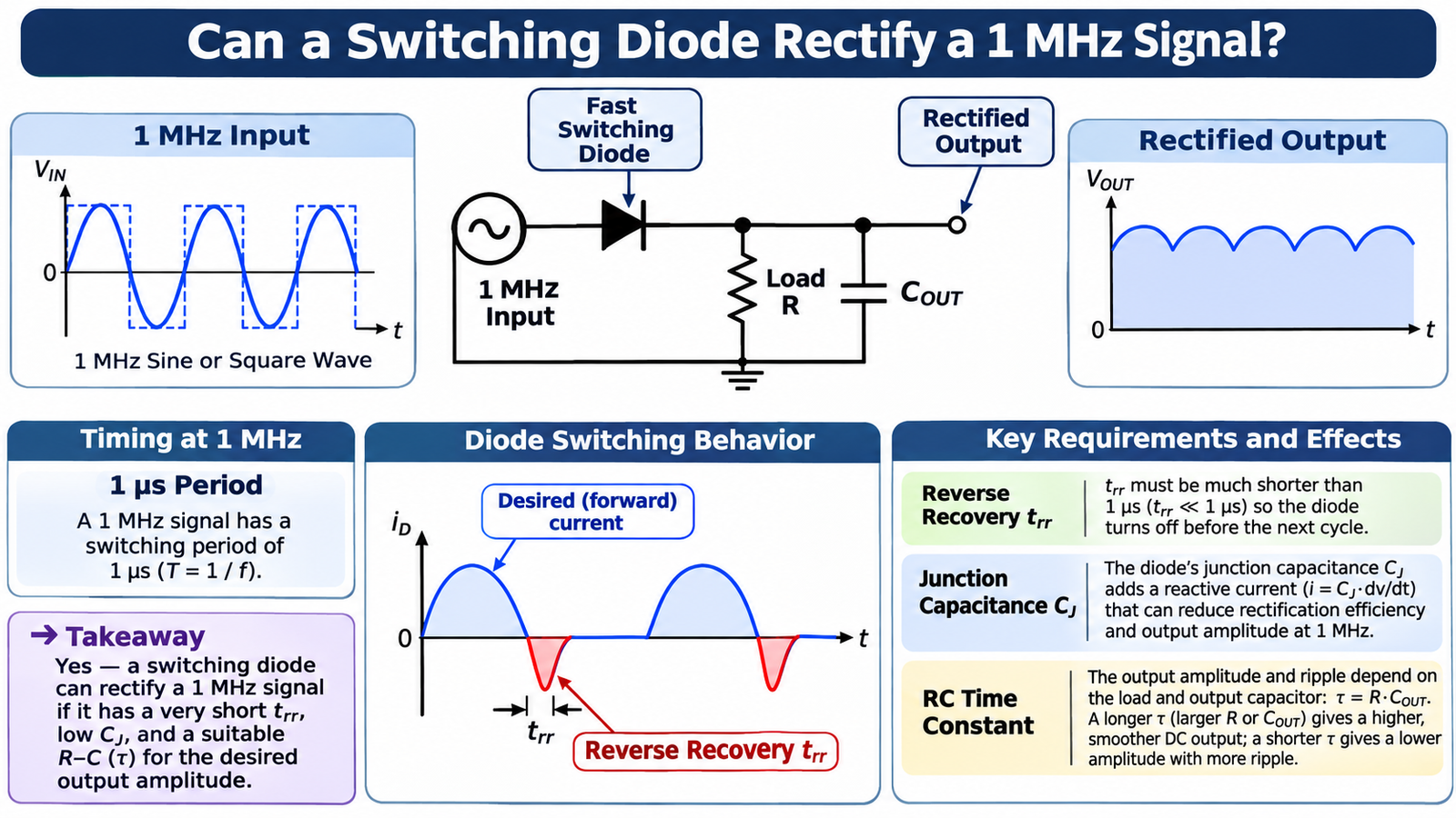
Yes. A switching diode can rectify a 1 MHz signal if its reverse-recovery time is far shorter than the 1 µs signal period and its junction capacitance, forward voltage, leakage and current ratings fit the source and load. The output RC network must also charge fast enough without loading the source, then hold the required voltage between peaks.
Translate 1 MHz into a timing requirement
The period is T = 1/f = 1 µs. In a half-wave detector the diode must stop conducting soon after the input reverses. A reverse-recovery time of a few nanoseconds occupies only a small fraction of the period, while a slow rectifier with microsecond-scale recovery may conduct into the wrong half-cycle and reduce output amplitude.
Do not select from the word “fast” alone. Read the reverse-recovery test current, reverse voltage and load resistance. A data-sheet number measured at 10 mA may not represent a different current or commutation slope.
Check four diode parameters
| Parameter | Effect at 1 MHz | Selection question |
|---|---|---|
| Reverse recovery trr | Creates reverse current and lost charge after polarity reversal | Is trr much shorter than the available off-time? |
| Junction capacitance CJ | Passes displacement current and loads a high-impedance source | Is reactance high enough at 1 MHz? |
| Forward voltage VF | Reduces detected amplitude, especially for small signals | Will the input peak exceed VF with margin? |
| Reverse leakage IR | Discharges the hold capacitor and creates error | Is leakage acceptable at maximum temperature? |
Junction-capacitance reactance is approximately XC = 1 / (2πfCJ). At high source impedance, even a few picofarads can influence gain and phase. This is why a small-signal switching diode and a power rectifier with similar voltage ratings can behave very differently. Start with the selection framework in rectifier diode fundamentals.
Choose the output RC time constant
For an envelope or peak detector, the capacitor should charge during a short conduction interval and discharge slowly enough through the load to limit droop. A first approximation is τ = RLOAD × COUT. A larger τ reduces ripple but slows response to falling amplitude and can demand higher peak diode current. A smaller τ follows modulation faster but produces more droop.
The source resistance, diode dynamic resistance and capacitor ESR also affect charging. Simulate the complete source, diode, load and probe, then verify the real waveform.
Switching diode or Schottky diode?
A small PN switching diode can offer low capacitance, low leakage and nanosecond recovery. A Schottky diode has no minority-carrier recovery and usually lower forward voltage, but reverse leakage can be higher and temperature-sensitive. The best choice depends on signal amplitude, source impedance, reverse voltage and acceptable leakage—not frequency alone.
The familiar 1N4148 is a PN switching diode, not a Schottky device, as explained in the 1N4148 classification guide. Compare its behavior with Schottky diode operation before substituting one for the other.
Validate the rectifier at 1 MHz
- Drive the circuit from a source with known amplitude and source resistance.
- Measure input and output with short connections and a probe whose capacitance is included in the design.
- Test the minimum expected input amplitude, not only a large laboratory signal.
- Check output ripple, recovery time and settling after amplitude changes.
- Repeat at minimum and maximum temperature to expose leakage error.
For precision detection, compare the passive diode result with an active or synchronous rectifier. At very low amplitude, an op-amp precision rectifier may avoid the forward-drop problem, provided its gain bandwidth and slew rate are sufficient.
Estimate whether the source can charge the capacitor
During each peak, capacitor charging current is limited by source resistance, diode resistance and wiring inductance. A large capacitor may improve hold-up yet require a narrow, high-amplitude charging pulse. Check the diode’s peak current rather than only the load’s average current. For a sine input, conduction begins only when the instantaneous input exceeds the capacitor voltage plus VF, so the available charging interval can be much shorter than half a cycle.
If the source is a logic pin, sensor or RF network, the rectifier may distort the source waveform. Buffer it or reduce capacitance when source loading changes the quantity being measured.
Design with frequency margin rather than validating at exactly 1 MHz only. Clock tolerance, harmonic-rich square waves and future frequency changes can shorten the commutation interval. Test above the highest specified frequency and include the fastest input edge, because dV/dt-driven capacitive current depends on edge speed as well as repetition rate.
Selection checklist
- VRRM exceeds the maximum reverse peak with margin.
- Peak and average forward current ratings cover capacitor charging.
- trr is comfortably shorter than the commutation interval.
- CJ is acceptable for the source impedance at 1 MHz.
- VF and leakage meet the amplitude-error budget.
- The RC network meets both ripple and response-time requirements.
Review MOT’s small-signal switching diodes and small-signal Schottky diodes against the actual waveform and temperature limits.