
Drive a P-channel MOSFET from the gate-to-source voltage, not gate voltage to ground. Pull the gate up to the source to turn the device off; pull the gate below the source to turn it on. When the source sits above the logic rail, use a transistor or driver as a level shifter, add a gate-to-source pull-up, and clamp |VGS| below the absolute maximum rating.
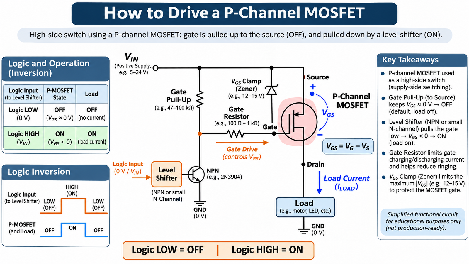
Read every voltage from the source terminal
For a P-channel MOSFET, VGS = VG − VS. The device is off when VGS is near 0 V and turns on as VGS becomes negative. If the source is at +12 V and the gate is at +12 V, VGS is 0 V. Pulling the gate to +7 V produces VGS = −5 V.
Gate threshold is only the beginning of conduction. Select a gate voltage for which the data sheet specifies RDS(on). The operating principle is covered in how a P-channel MOSFET works.
Use a defined default-off network
Place a resistor from gate to source so the MOSFET remains off when the controller is unpowered, disconnected or resetting. The resistor must be low enough to overcome leakage and noise but high enough to avoid unnecessary current when the level shifter holds the gate low.
A small NPN transistor or N-channel MOSFET can pull the P-channel gate downward. The logic becomes inverted: an active level-shifter input turns the P-channel device on. Check startup sequencing; a floating or partially powered level shifter can otherwise create an unintended pulse.
Protect the gate from excessive negative VGS
Pulling a gate to ground is unsafe when the source bus exceeds the MOSFET’s allowed |VGS|. For example, a 24 V source and a grounded gate would demand VGS = −24 V. Add a gate-to-source Zener or dedicated clamp and design the pull-down current so the clamp stays within its current and power limits.
The clamp protects the oxide, but it does not replace transient control on the drain or source rail. Apply the broader methods in MOSFET gate protection.
Choose the gate resistor from charge and switching loss
A MOSFET gate draws little steady-state current, yet it requires current to charge and discharge its gate charge QG. A first estimate of average driver current is IG,AVG = QG × fSW. The peak current needed for a transition is approximately IG ≈ QGD / tMiller for the Miller interval.
The total series resistance includes driver output resistance, the external resistor and the MOSFET’s internal gate resistance. Faster transitions reduce overlap loss but increase ringing, dV/dt and EMI. Slower transitions reduce EMI but increase switching loss. Validate both edges at line, load and temperature.
High-side load switch versus high-frequency PWM
| Use | Typical drive priority | Main check |
|---|---|---|
| Static load disconnect | Simple level shift and safe default state | Inrush, reverse current and SOA |
| Low-frequency PWM | Moderate gate current | Thermal rise during repeated edges |
| High-frequency conversion | Strong source-referenced driver | Gate charge, switching loss and dead time |
P-channel devices simplify high-side drive but usually have higher RDS(on) than an equivalent-size N-channel device. At high current or switching frequency, an N-channel MOSFET with a bootstrap, charge-pump or isolated driver may be more efficient.
Illustrative 12 V logic-interface example
For a 12 V source controlled by 3.3 V logic, connect the P-channel source to 12 V and use a gate-to-source pull-up for off. A small level-shift transistor can pull the gate downward for on. Do not assume the gate should reach ground: choose the pull-down and clamp so the on-state VGS is strong enough for the specified RDS(on) but remains within the gate rating. Then calculate pull-up current, clamp current and transistor dissipation for the full source-voltage range.
Measure VGS with the probe referenced to the source pin. A ground-referenced gate trace alone can look correct while source bounce produces an unsafe or insufficient actual VGS.
Connect and validate the circuit
- Confirm source, drain and gate pinout for the exact package.
- Connect the source to the positive rail and drain to the load for the intended high-side direction.
- Add the gate-to-source pull-up before connecting the level shifter.
- Add gate resistance and a VGS clamp when required.
- Power up with a current-limited source and verify VGS directly at the MOSFET pins.
- Measure VDS, load current, transition time and temperature under worst-case load.
For related low-side, high-side and back-to-back connections, use the diagrams in how to wire a MOSFET. For selection, compare voltage margin, current, RDS(on), QG and thermal resistance using the MOSFET selection guide.
Common mistakes
- Using gate-to-ground voltage instead of VGS.
- Leaving the gate floating during reset.
- Pulling the gate to ground on a bus that exceeds |VGS|max.
- Using VGS(th) as the fully-on voltage.
- Ignoring body-diode current, inrush and reverse-current paths.
Browse MOT’s power MOSFETs only after the complete gate-drive and thermal conditions are defined.