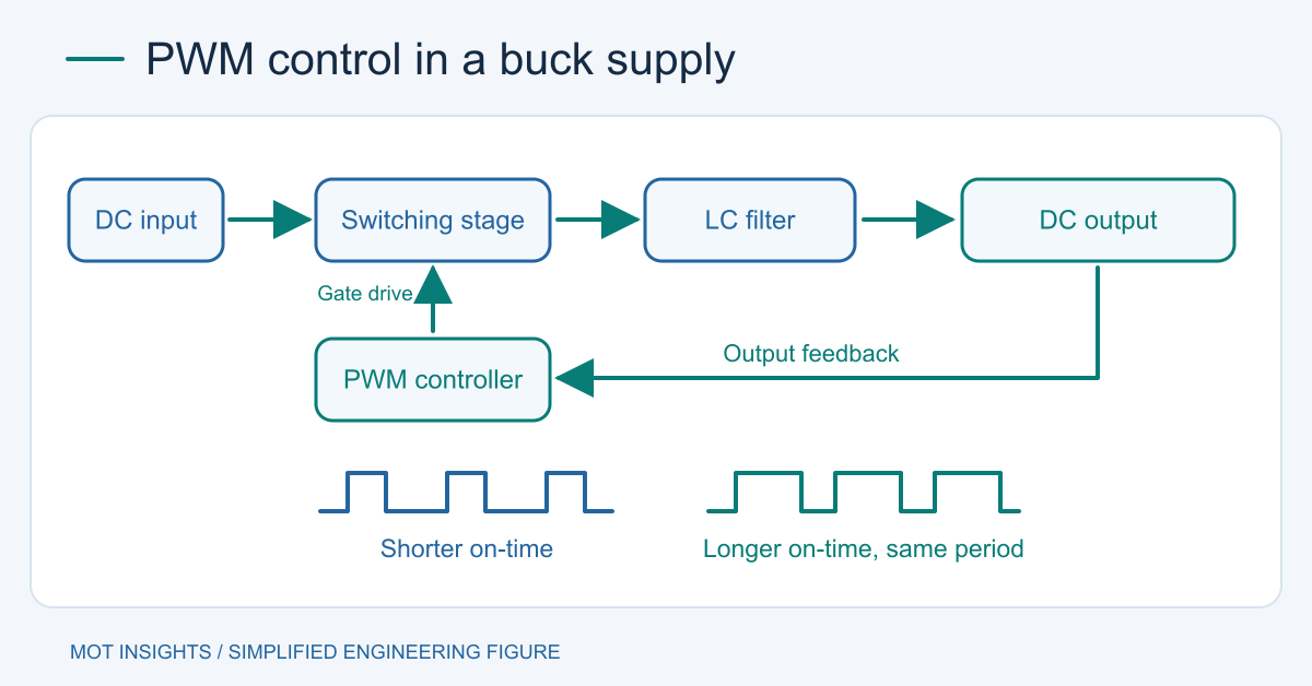
A PWM switching power supply regulates its output by changing how long a power switch stays on during each switching period. The switch sends pulses into an energy-storage stage, and the output filter delivers DC with residual ripple. In a fixed-frequency regulator, the pulses can get wider or narrower while the period stays the same. PWM stands for pulse-width modulation.
What the controller changes
Duty cycle is the fraction of a period during which the controlled switch is on: D = ton ÷ T = ton × fsw. At 200 kHz, T is 5 µs. A 2 µs pulse represents 40% duty cycle. Use the high-side switch on-time for the buck example below. A feedback node samples the output through a divider and compares it with a reference. When the output dips, the control loop adjusts pulse width or its current command to restore regulation. The detailed timing depends on the controller architecture.
A voltage-mode controller can compare an amplified output error with an oscillator ramp. In a typical peak-current-mode controller, the output error establishes a target for inductor or switch current, and the sensed current helps end the on-pulse. Both can use PWM. A controller may also override the normal command for an overcurrent, startup ramp or input undervoltage. See how a switching power supply works to place the controller, power stage and protection blocks in the complete supply.
Worked example for a 12 V to 5 V buck
An ideal buck operating in continuous conduction and steady state has Vout ≈ D × Vin. At 12 V input and 5 V output, D ≈ 41.7%. At 200 kHz, this corresponds to 2.08 µs of high-side on-time. If Vin rises to 15 V with the same output target, the ideal duty falls to about 33.3% and on-time to 1.67 µs.
During on-time, the inductor sees approximately Vin − Vout and its current rises. During off-time, current freewheels through the diode or low-side synchronous switch and ramps down. The average inductor voltage over a settled cycle is zero. This volt-second balance produces the ideal buck relationship. Losses in the switches, inductor and interconnect shift the real duty cycle. A boost converter or isolated flyback has a different conversion equation. Switch-mode power supply design
What changes on the bench
| Observation | Possible explanation | What to check |
|---|---|---|
| Pulses narrow as Vin rises | Normal fixed-frequency buck regulation | Vout remains near its target |
| Output droops and duty stops increasing | Maximum duty, input sag or a current limit | Vin at the converter, inductor current and controller status |
| Pulses occur in bursts at light load | Controller enters a light-load efficiency mode | Mode settings, ripple and average switching rate |
| Successive current peaks alternate | Possible current-loop instability under certain peak-current-mode conditions | Current sense, slope compensation and operating duty |
At high input voltage and low output voltage, the required pulse can be shorter than the controller’s minimum on-time. At low input voltage, a buck may run out of duty cycle before it reaches the target. If an inductor saturates, current can rise quickly even though the pulse width looks reasonable. Observe the load and sense waveform before changing the feedback circuit.
How to verify duty cycle and output ripple
On a documented low-voltage DC/DC bench setup, measure Vin and Vout at the board under the same load. Measure switch-node pulse width using a probe and grounding method appropriate to the board. If you need the high-side gate drive, measure gate to source with the suitable differential arrangement. A gate reading relative to board ground can misrepresent the voltage that controls a floating high-side MOSFET. Keep the ripple probe loop short and capture both individual switching cycles and slower load transients. Measuring switch-mode supply ripple
Repeat the measurements at minimum and maximum input and at representative loads. Duty cycle and efficiency are different quantities. A 41.7% duty ratio can coexist with much higher efficiency because the duty ratio describes timing, while efficiency compares output and input power. Include both voltages and currents when measuring power supply efficiency.
Frequently asked questions
Does PWM mean the output is a square wave?
The square wave is usually at a gate or switch node. The output filter and control loop produce the regulated DC rail. Ripple and load-transient excursions are separate specifications.
Why does switching frequency change at light load?
Some controllers reduce energy loss by skipping pulses, entering burst operation or changing frequency. Check the mode pin and controller documentation before interpreting a different pulse pattern as a fault.
If duty and ripple are within specification but losses are high, use the measured voltage, current and switching frequency when selecting a buck-converter MOSFET.