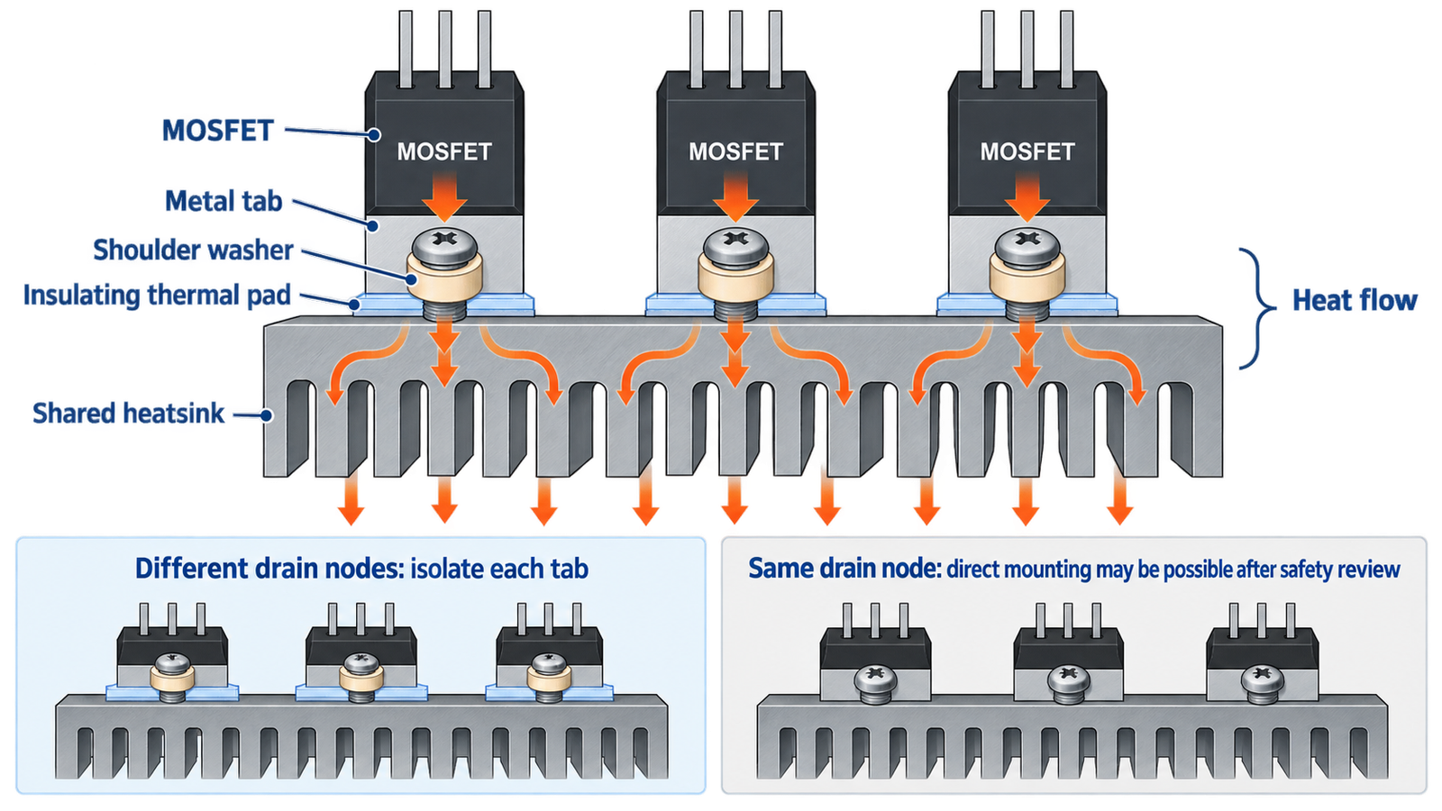
Yes, multiple MOSFETs can share the same heatsink, and this is common in inverters, motor drives, audio amplifiers, and power supplies. The arrangement is safe only when the heatsink can remove the combined heat and the metal mounting surfaces cannot create an unintended electrical connection. In many leaded power packages, the exposed tab is connected to the drain, so bolting devices directly to one conductive heatsink may short together circuit nodes that must remain separate.
A shared heatsink is therefore both a thermal component and a possible conductor. Treat its electrical potential, insulation system, mechanical stack, airflow, and temperature distribution as deliberate parts of the design.
Why sharing one heatsink can work
A heatsink does not care which transistor supplied the heat. If three MOSFETs dissipate 8 W, 10 W, and 12 W, the sink must ultimately reject about 30 W, plus any heat from nearby components that couples into it. A single larger sink can use space and airflow more efficiently than several small sinks. It can also simplify mechanical construction and make device case temperatures more similar.
Those benefits do not make every shared mounting arrangement correct. The designer must answer two separate questions: are the devices electrically allowed to touch the same metal, and will every junction stay below its allowable temperature under the worst credible load and ambient condition?
Check the package tab connection first
For many TO-220, TO-247, D2PAK, and related MOSFET packages, the exposed metal tab is internally connected to the drain. The exact connection is package- and manufacturer-specific, so confirm it in the datasheet. If MOSFETs occupy different half-bridge nodes, their drains switch between different voltages. Directly bolting both bare tabs to the same uninsulated heatsink creates a short circuit.
Use an electrically insulating thermal interface under each device when the tabs cannot share a potential. Common choices include silicone pads, ceramic-filled pads, mica with approved compound, or an isolated package such as a full-pack device. The screw may also need an insulating shoulder washer so its shank and head cannot bridge the tab to the sink. Check the pad’s dielectric rating, thickness, thermal resistance, puncture resistance, aging, and mounting requirements.
Even when all drains are intentionally common, direct mounting deserves a safety review. The heatsink may become electrically live at the drain voltage. It then needs the required enclosure, protective bonding or isolation strategy, creepage, clearance, touch protection, and fault analysis. A black-anodized finish is not a certified electrical insulator.
Build the thermal-resistance model
The basic steady-state path for each MOSFET is junction to case, case through the interface material to the heatsink, and heatsink to ambient. Estimate the junction temperature of device i with:
TJ,i = TS,local + Pi × (RθJC,i + RθCS,i)
The local sink temperature is not always the same everywhere. A first estimate for the overall sink rise is total dissipated power multiplied by heatsink-to-ambient thermal resistance. Then add local spreading resistance or use simulation and measurement when devices are crowded, the heat source is small, or airflow is uneven.
The article on how to calculate heatsink size for a MOSFET explains the resistance-chain method in more detail. For a shared sink, replace the single-device heat load with the sum of simultaneous losses, while still checking each device’s individual junction-to-case and interface rise.
Calculate realistic MOSFET loss
Do not rate the sink from current alone. MOSFET heat includes conduction loss, switching loss, body-diode or third-quadrant loss, reverse-recovery interaction, gate-drive loss that may heat the driver, and any avalanche or linear-mode energy. On-resistance rises with junction temperature, so conduction loss should use the hot RDS(on) value rather than the headline room-temperature value.
Switching loss depends on bus voltage, current, transition time, gate resistance, driver strength, package inductance, and switching frequency. If the application uses parallel devices, dynamic current may not divide equally. The primer on why MOSFETs get hot helps identify the loss mechanisms before the thermal calculation begins.
Account for thermal interaction
Heat from one MOSFET raises the base temperature seen by its neighbors. This mutual heating is beneficial only if it equalizes devices that already share current safely. It can be harmful when one switch has much higher duty cycle, sits in a stagnant airflow region, or is clustered near another hot component.
Place devices far enough apart for mounting hardware, creepage, service access, and heat spreading. More spacing generally lowers peak base temperature, but it increases busbar or trace length. The best layout balances thermal spreading with low-inductance power and gate loops. In a fast half bridge, do not stretch the commutation loop merely to reach a remote heatsink position.
A forced-air sink must be evaluated with the real fan, duct, dust filter, orientation, and inlet temperature. The downstream device may receive air already warmed by upstream fins. Natural-convection ratings also depend strongly on fin direction and free space around the sink.
Choose the interface material carefully
Electrical isolation adds thermal resistance. A thicker pad can withstand more mechanical variation and sometimes more voltage, but it usually increases junction temperature. A thin high-conductivity pad may perform better thermally but require a flatter surface and controlled assembly.
Use only enough thermal compound to fill microscopic voids. Excess paste is not a substitute for flat surfaces and can increase bond-line thickness. Avoid mixing a dry pad with grease unless the pad supplier specifies that combination. Confirm whether the published RθCS assumes a particular pressure, surface finish, or test coupon.
Mount all devices consistently
- Deburr and clean the heatsink mounting surface.
- Position the approved insulation pad without folds, tears, trapped debris, or metal chips.
- Fit the shoulder washer and other hardware in the documented order.
- Tighten with the package manufacturer’s recommended torque and sequence.
- Do not use the screw to force a misaligned leaded package into position.
- After assembly, inspect pad coverage and check electrical isolation before power is applied.
Too little pressure raises contact resistance; too much can crack the package, extrude the pad, bow the heatsink, or damage insulation. Spring clips often provide more repeatable long-term force than individual screws, but only when designed for the package and sink geometry.
What if the MOSFETs are connected in parallel?
Parallel MOSFETs in the same switch position often have common drains, making a shared sink electrically easier. They still need symmetrical source and drain paths, individual gate resistors, matched gate-loop inductance, and suitable Kelvin-source connections. Positive RDS(on) temperature coefficient helps steady-state sharing, but it does not guarantee equal switching current.
For the gate and power connections, see how to wire a MOSFET. Measure individual current or infer it from carefully placed low-inductance sensors during switching tests. One device can carry a disproportionate transient current while the average case temperatures appear similar.
Verify the design on real hardware
Start with insulation resistance or dielectric testing appropriate to the voltage class and applicable standard. Then power the assembly from a current-limited setup and increase load gradually. Measure sink temperature near each device, case temperature using a corrected method, and junction temperature by a validated electrical or thermal model.
Thermal cameras can miss shiny metal surfaces or show the pad rather than the junction. Add high-emissivity measurement spots where permitted and correlate them with thermocouples. Run the worst ambient temperature, lowest airflow, highest switching frequency, overload profile, and component tolerances. Also test a stalled or failed fan if that is a credible fault.
Keep margin below the absolute maximum junction temperature. Reliability usually improves substantially when the normal junction temperature and temperature swing are reduced. The site’s guide to the PCB thermal path for power MOSFETs is useful when the board and copper planes share part of the cooling work.
When separate heatsinks are better
Use separate sinks when electrical isolation would add too much thermal resistance, the switch nodes have demanding creepage requirements, devices dissipate very different power, or the physical layout would create long high-current loops. Separate sinks also make some prototypes easier to probe and may reduce capacitive common-mode current from switching tabs to a large chassis-connected surface.
A shared sink is often the best production solution, but only after thermal and electrical constraints are solved together. The decisive question is not whether several MOSFETs fit on one piece of aluminum. It is whether every device remains electrically isolated where required and stays within its junction-temperature limit in the assembled system.
Frequently asked questions
Can MOSFET tabs touch the same heatsink?
Only if the datasheet confirms the tab connection and the circuit permits all tabs and the heatsink to share that potential. Otherwise use approved electrical insulation.
Should I add the wattage of all MOSFETs?
Yes, use the simultaneous total loss to estimate sink-to-ambient temperature rise, then check each MOSFET’s local junction-to-case and case-to-sink rise.
Can one thermal pad cover several MOSFETs?
It can if the material, thickness, pressure, creepage, and puncture performance are approved for the assembly. Individual pads are often easier to inspect and replace.
Does anodizing electrically isolate a heatsink?
Do not rely on ordinary anodizing as the safety insulation system. Scratches, mounting hardware, edges, and process variation can defeat it.