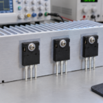
Yes, MOSFETs get hot. A working MOSFET is never an ideal switch, so part of the electrical energy becomes heat. A moderate, predictable temperature rise can be normal. Rapid heating, thermal shutdown, discoloration, or repeated failure indicates excessive loss, an inadequate thermal path, or operation outside the device’s ratings.
The useful question is not whether the package feels warm. It is whether the semiconductor junction remains below its allowed temperature with sufficient margin in the worst combination of current, switching frequency, ambient temperature, and cooling.
Why does a MOSFET get hot?
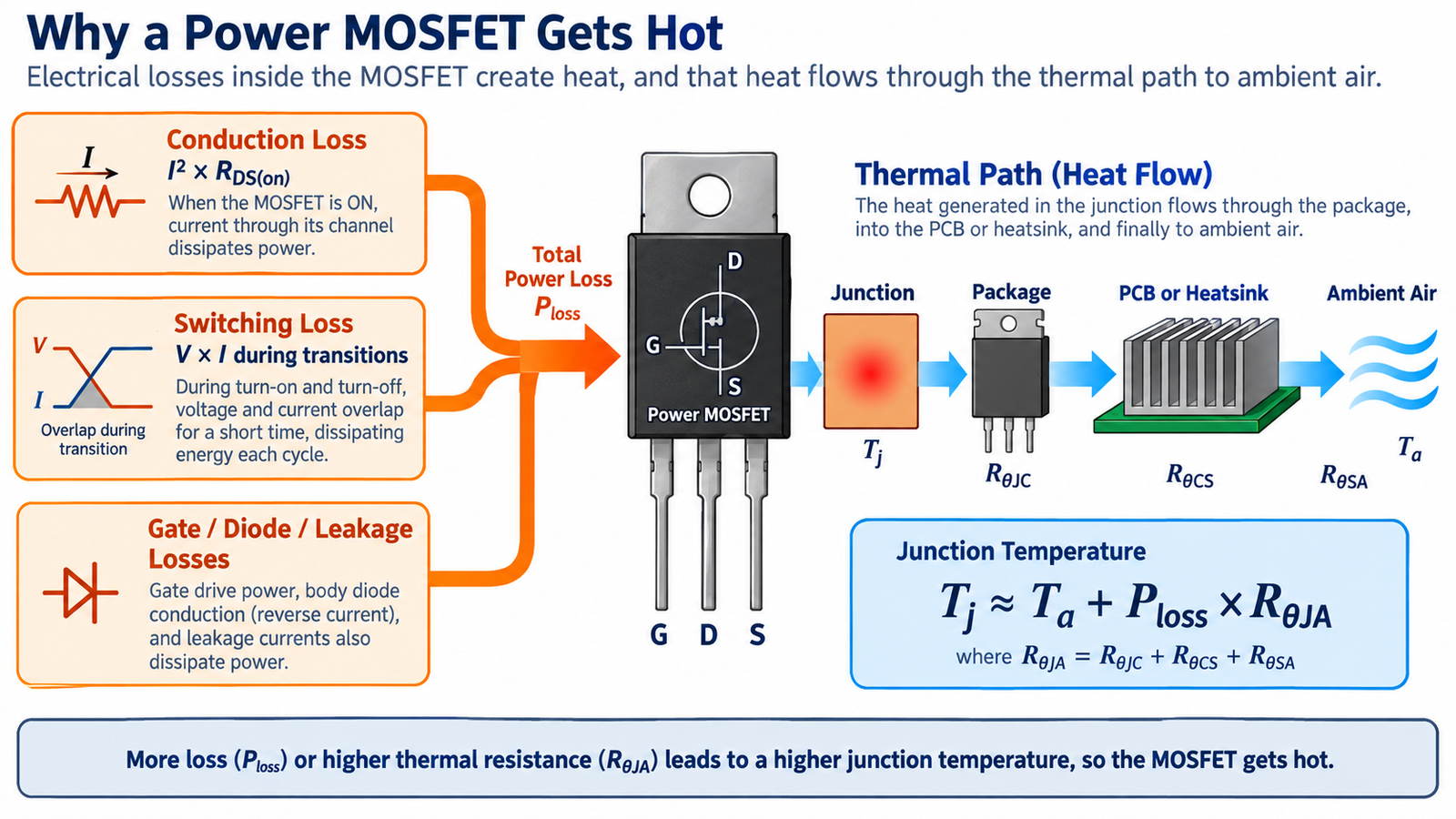
Conduction loss
When the device is fully on, it behaves approximately like a small resistance. For a steady current, conduction loss is P = I² × RDS(on). In PWM circuits, use RMS current and duty cycle. RDS(on) increases with junction temperature, sometimes substantially, so calculate with the datasheet’s temperature-normalized value rather than only the 25 °C specification.
A MOSFET that looks excellent at low current can still dissipate several watts at high current because current is squared. Connection, lead, solder, and PCB resistance may add local heating that is incorrectly blamed on the silicon.
Switching loss
During turn-on and turn-off, drain voltage and drain current overlap. The energy lost per transition multiplied by switching frequency becomes switching power. Slow gate drive, high gate resistance, Miller plateau duration, common-source inductance, and large parasitic capacitance can extend the overlap.
Driving the gate faster can reduce switching loss, but it may increase ringing, overshoot, and electromagnetic interference. The goal is a controlled transition, as explained in the guide to tuning a MOSFET gate resistor for efficiency and EMI.
Other losses
- Body-diode conduction: dead time or reverse current can force current through the diode, which usually has a larger voltage drop than the channel.
- Reverse recovery and output capacitance: charge moved during commutation can heat both MOSFETs in a half bridge.
- Gate-drive power: repeatedly charging total gate charge consumes driver power and contributes some device-related loss.
- Linear operation: a MOSFET used as a pass element can have high voltage and current simultaneously. Safe operating area becomes critical.
- Leakage and avalanche: normally smaller, but they can become important at high temperature or during repetitive transients.
How hot is too hot?
The maximum junction temperature in the datasheet is an absolute limit, not a recommended design target. Many silicon power MOSFETs list a maximum around 150 °C or 175 °C, but the exact value depends on the device. Reliability generally improves when the normal operating junction temperature stays well below that limit and transient margin remains.
Touch is not a valid measurement. A metal tab or heatsink hot enough to burn skin may still correspond to an acceptable junction temperature in one design, while a package that feels only warm may hide a much hotter die if the internal or board thermal path is poor.
Estimate the junction temperature
For a first steady-state estimate, use Tj ≈ Ta + Ploss × RθJA when the datasheet’s junction-to-ambient condition resembles the real board. If the device is attached to a heatsink, model the path in parts: junction-to-case, case-to-interface or sink, and sink-to-ambient. Use the applicable thermal resistance, not whichever number is smallest.
Datasheet RθJA often comes from a defined test PCB. Copper area, layer count, thermal vias, airflow, nearby heat sources, and enclosure temperature can make the real result very different. The article on PCB thermal paths for power MOSFETs explains how heat actually leaves surface-mount packages.
Signs of abnormal MOSFET heating
- The temperature rises quickly even at light load.
- One device in a parallel bank is much hotter than the others.
- The circuit works at startup but fails after several minutes.
- Waveforms show a slow Miller plateau, oscillation, cross-conduction, or excessive dead time.
- The PCB, solder joint, or connector is hotter than the package.
- Thermal protection cycles repeatedly or RDS(on)-related voltage drop increases sharply.
A single hot device can indicate current imbalance, mismatched gate resistors, unequal source inductance, poor soldering, or a damaged die. Do not assume that adding airflow fixes the electrical cause.
How to reduce MOSFET temperature
- Calculate every important loss term. Separate conduction, turn-on, turn-off, diode, output-capacitance, and gate-drive losses.
- Select for the real operating point. Check voltage margin, hot RDS(on), gate charge, switching energy, package, and safe operating area. The practical MOSFET selection guide provides a structured method.
- Use an adequate gate driver. Confirm peak source and sink current, gate voltage, UVLO behavior, dead time, and high-side drive.
- Reduce loop inductance. Keep gate and commutation loops short and provide a clean Kelvin source return when the package supports it.
- Improve the thermal path. Add copper area, thermal vias, an exposed pad, interface material, a heatsink, or forced airflow as appropriate.
- Measure under worst case. Test high line, low line, maximum load, maximum ambient, startup, short transients, and abnormal conditions.
Common design mistakes
Gate threshold voltage is often misused as the recommended drive voltage. VGS(th) is measured at a small current and only indicates the start of channel formation. Use the RDS(on) test voltage or the manufacturer’s recommended drive condition to turn the device fully on.
Another mistake is treating the datasheet current rating as a usable board current. That rating may assume an ideal case temperature and does not automatically account for package leads, PCB copper, duty cycle, switching loss, or connector limits. For linear or surge operation, verify the MOSFET safe operating area.
Frequently asked questions
Should a MOSFET be cool when fully on?
Not necessarily. Low RDS(on) reduces conduction loss, but a high-current device can still dissipate meaningful power. Switching and diode losses may dominate in a converter.
Does a hotter MOSFET conduct better?
For a silicon MOSFET in the fully enhanced region, RDS(on) usually increases with temperature, so conduction loss rises. Temperature behavior in the linear region is more complex and must be checked against safe operating area.
Can I test MOSFET temperature with an infrared camera?
Yes, with care. Emissivity, reflective metal tabs, viewing angle, and inaccessible junction temperature affect accuracy. Apply high-emissivity tape or coating at a safe measurement point and correlate case temperature with a thermal model.
Will a bigger heatsink always solve the problem?
No. A heatsink cannot correct cross-conduction, insufficient gate voltage, excessive switching time, avalanche, or an overloaded device. Reduce electrical loss first, then size the cooling system.