GaN power transistors drive high-performance LiDAR by switching large laser-diode currents on and off within a few nanoseconds. Their low charge, low capacitance, small package, and ability to tolerate very high repetitive pulse current let the transmitter create a narrow, bright optical pulse without a large, slow power stage.
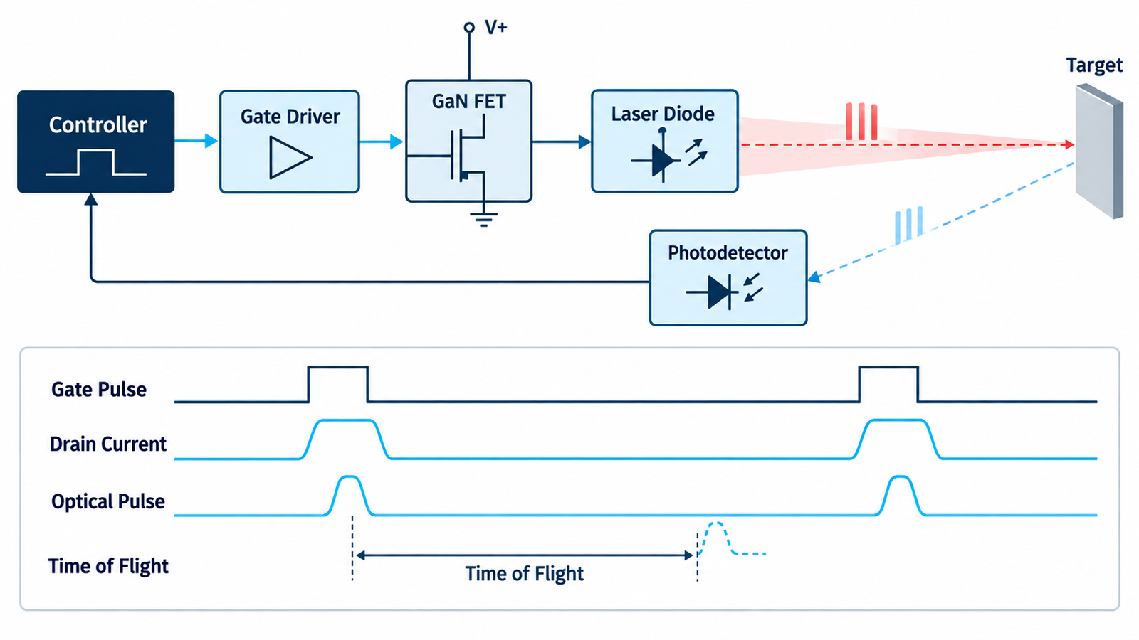
In a direct time-of-flight system, the transmitter sends a light pulse and the receiver measures how long the reflection takes to return. The distance is proportional to half the round-trip time multiplied by the speed of light. The electrical switch therefore affects optical pulse shape, ranging precision, maximum distance, receiver filtering, electromagnetic interference, and thermal load. Engineers who need a wider power-conversion background can first review how a power transistor switches current.
Why pulse width matters in LiDAR
A shorter optical pulse occupies a smaller distance interval. In ideal timing, 1 ns of round-trip time corresponds to about 15 cm of one-way distance. Actual resolution also depends on detector bandwidth, timing jitter, signal processing, target reflectivity, atmospheric loss, and pulse shape. A fast switch does not guarantee centimeter accuracy by itself, but it prevents the transmitter from being the dominant source of pulse broadening.
Peak optical power helps reflections rise above detector noise and sunlight. The laser current may be tens or hundreds of amperes even though the average current is modest, because the pulse is extremely short and the duty cycle is low. The design must stay inside the laser diode’s pulsed-current, junction-temperature, and optical-safety limits rather than treating a spectacular oscilloscope peak as continuous capability.
Why GaN is well suited to the laser driver
- Low gate charge: the driver can change the channel state rapidly without moving as much charge as a larger silicon MOSFET may require.
- Low output capacitance: less stored energy must be charged and discharged on each event.
- Small packages: chip-scale GaN devices can sit close to the laser diode and pulse capacitor, shrinking the high-current loop.
- Fast voltage transition: a clean transition helps create narrow pulses and reduces overlap between voltage and current.
- Repetitive pulse capability: a correctly selected device can deliver high peak current at a low duty cycle, subject to transient thermal and reliability limits.
These benefits are different from saying that GaN has no loss. The transistor still has conduction loss, capacitive loss, gate-drive loss, and energy associated with ringing. The best comparison uses measured electrical and optical waveforms in the intended circuit, not only headline RDS(on). For general selection tradeoffs, see why power transistors get hot.
The basic GaN LiDAR pulse circuit
A controller or timing IC sends a logic pulse to a high-current gate driver. The driver quickly changes the GaN gate voltage. When the FET turns on, energy stored in a local capacitor flows through the laser diode and the transistor. The path may be a simple hard-switched loop or a resonant network that deliberately shapes current. The photodetector and time-to-digital converter then record the return.
The loop containing the storage capacitor, laser diode, GaN FET, and return copper must be extremely small. An inductance of only a few nanohenries can create substantial overshoot when current changes by tens of amperes per nanosecond. Package choice, component placement, wide overlapping copper, short vias, and a low-inductance capacitor are therefore part of the switch design.
Gate-drive requirements
Enhancement-mode GaN devices normally use a lower gate voltage and have a smaller absolute gate-voltage margin than conventional silicon MOSFETs. The driver should be close to the transistor, its supply must be well bypassed, and source inductance shared by the power and gate loops should be minimized. Separate gate resistors for turn-on and turn-off can help tune edge speed, but resistance alone cannot correct a poor current-loop layout.
A passive probe with a long ground lead can invent ringing that is not present or hide ringing that is. Use a high-bandwidth differential or coaxial probing method, a current sensor with adequate rise time, and optical measurement equipment that can resolve the laser pulse. The same discipline used to control MOSFET gate resistance, efficiency, and EMI applies here, but the nanosecond time scale makes parasitics even more critical.
What limits range and image quality
Increasing current is not a universal route to longer range. The laser may saturate or exceed its pulsed rating, the optical system may clip, the FET voltage may overshoot, and the receiver can be blinded by close reflections. Atmospheric attenuation and target reflectivity set limits that the transistor cannot overcome. Multi-channel systems also need low channel-to-channel skew so adjacent pixels do not receive different pulse energy or timing.
Pulse-to-pulse repeatability matters because the ranging algorithm estimates timing from many returns. Supply droop, temperature-dependent laser efficiency, gate-driver jitter, and resonant-loop tolerance all move the waveform. A useful validation plan records peak current, optical power, pulse width, ringing, delay, jitter, and temperature over voltage, ambient, repetition rate, and lifetime.
Thermal and reliability design
Low duty cycle reduces average heat, but the junction experiences a rapid temperature impulse. Use the datasheet transient thermal impedance, not only steady-state thermal resistance. Confirm that the repetitive pulse sequence allows the junction to cool and that the laser and capacitor have adequate ripple-current life. Copper spreading and thermal vias can help, although electrical loop area must stay small.
Fast edges can couple noise into the detector, timing circuit, vehicle network, and enclosure. Partition transmitter and receiver returns, manage common-mode current, shield sensitive nodes, and evaluate radiated emissions with the optics operating. A broader PCB thermal-path design guide helps translate device loss into board temperature.
Practical design workflow
- Define wavelength, required range, field of view, repetition rate, pulse width, detector sensitivity, and eye-safety class.
- Select a laser diode with pulsed-current and thermal data for the intended pulse duration.
- Choose a GaN FET with adequate voltage margin, peak-current capability, low charge, and a package that enables a small loop.
- Select the topology and calculate initial storage capacitance or resonant elements.
- Place the pulse capacitor, laser diode, FET, and return before routing any low-current control signals.
- Simulate parasitic inductance and capacitance, then validate them with double-pulse or dedicated laser-driver measurements.
- Tune the gate drive while watching voltage overshoot, optical waveform, EMI, and driver temperature.
- Run temperature, voltage, repetition-rate, aging, and fault tests, including open-laser and shorted-node conditions.
Frequently asked questions
Does a faster GaN transistor automatically increase LiDAR range?
No. It can produce a narrower and potentially higher peak pulse, but range also depends on laser efficiency, aperture, optics, detector sensitivity, background light, target reflectivity, atmospheric loss, and safety limits.
Why is the GaN FET placed so close to the laser diode?
Close placement minimizes high-current loop inductance. Lower inductance reduces overshoot and ringing and helps the electrical pulse remain narrow.
Can a normal silicon MOSFET drive LiDAR?
Yes, especially at moderate current or longer pulse widths. GaN becomes attractive when the application needs very fast, repeatable edges, compact layout, and high peak current.