Choose a boost converter MOSFET for the maximum output voltage plus switch-node overshoot, the inductor’s worst-case peak and RMS currents, and the loss at the available gate drive. In a conventional boost, the main MOSFET conducts input-side inductor current during its on interval. Low input voltage at high output power is often the first corner to check.
Translate operating conditions into switch current
Start with VIN,min and VIN,max, the maximum regulated output voltage, maximum output power, minimum expected efficiency, switching frequency, and the inductor’s hot inductance including tolerance. In continuous conduction, approximate average inductor current as POUT/(η × VIN), where efficiency η is a fraction. The ideal duty ratio D ≈ 1 − VIN/VOUT and ripple ΔIL ≈ VIN × D/(L × fSW) provide initial estimates. Correct these for real drops and timing as the design progresses.
As an example, a 60 W output from 10 V at 90% efficiency requires about 6.67 A average input current. Boosting to 24 V gives ideal D ≈ 0.583. With 10 µH and 300 kHz, ripple is about 1.94 A peak to peak and the estimated peak current is 7.64 A. A small inductance decrease during the pulse can increase that peak further. A peak-current controller’s limit also has tolerance and delay, which matter at startup and under overload.
Set VDS from the actual commutation loop
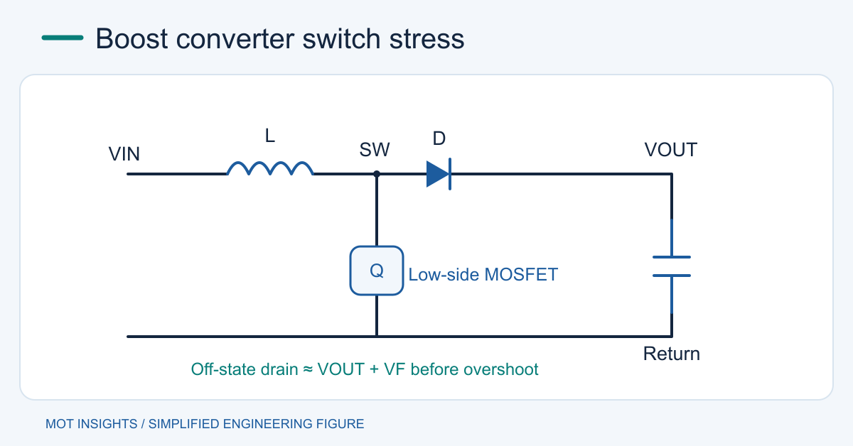
With the main MOSFET off, the switch node is near VOUT plus the diode’s forward voltage in an asynchronous stage. Stray inductance, diode recovery and output overshoot can raise the drain further. Check high output setpoint, load dump, startup and commutation at the worst current. Choose margin with measured waveforms and the product reliability requirement. An avalanche rating by itself does not establish that recurring spikes are acceptable. Review single-pulse and repetitive avalanche limits.
If the converter uses a synchronous rectifier, its high-side drive and body-diode behavior need a separate review. Check both turn-off paths and dead time. A synchronous stage can also conduct reverse current in some control modes, affecting startup into a prebiased output.
Balance channel, switching and drive losses
The main switch’s CCM RMS current is approximately √[D × (IL,avg² + ΔIL²/12)]. In the example it is about 5.11 A. With 12 mΩ hot on-resistance, conduction loss is about 0.31 W. Check the maximum RDS(on) at the actual gate bias, then account for temperature. Ensure the controller can source and sink the charge needed for the intended transitions, including Miller charge at the relevant drain voltage.
Compare overlap energy, output-capacitance energy and rectifier recovery. They vary with layout, temperature and transition speed. Estimate average driver supply power as Qg × Vdrive × fSW for a full charge cycle. That power is distributed in the gate path. For nonlinear output capacitance, use the manufacturer’s energy or charge curves at the actual voltage. Avoid counting a loss term twice if it is already included in measured switching energy.
Keep the current calculation consistent with the mode
The CCM equations assume that the inductor never fully discharges during the period. If the estimated current valley falls to zero, calculate from the controller’s discontinuous-conduction or pulse-skipping behavior. In a simplified discontinuous case where switch current ramps from zero to Ipk during on-time fraction D, its full-period RMS current is Ipk × √(D/3). Burst-mode measurements require a window long enough to include idle intervals. Peak stress can remain high even when average dissipation falls.
Review the input voltage range in both directions. Low line often dominates conduction loss, and higher line can change current-limit behavior, pulse width or gate timing. A supply that sometimes exceeds the target output voltage may require a different topology or a documented pass-through arrangement. Verify that the chosen boost controller handles that condition before selecting devices for it.
Verify operation before locking the footprint
Probe VGS and VDS at the device with suitable instrumentation, then measure inductor current at low line, high line and full load. Record turn-on and turn-off overshoot, minimum driver voltage and case temperature after thermal stabilization. Check light-load burst behavior separately. The switch-mode supply design guide covers layout, magnetics and loop validation.
An ordinary boost has a path from input through the inductor and output diode even when the switch is disabled. Check fault-current containment and output-disconnect requirements using the switching supply short-circuit guide. After capturing the real stress and gate drive, compare MOT power MOSFETs at equivalent conditions.