GaN is better than a SiC MOSFET in some high-frequency, high-power-density converters, but SiC is often better at higher voltage, higher power, and demanding thermal or fault conditions. Both are wide-bandgap semiconductor technologies. Their practical strengths overlap, so the answer depends on bus voltage, topology, switching frequency, load range, cooling, qualification, and total system cost.
A fair comparison uses real devices with the required voltage margin and package, driven in optimized circuits. Comparing one GaN data-sheet number with an unrelated SiC MOSFET can produce the wrong conclusion.
Where GaN usually has an advantage
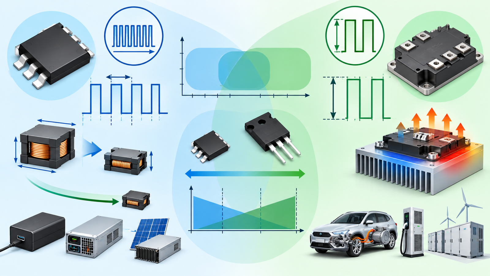
Power GaN devices commonly offer low gate charge, low output charge, small packages, and no conventional silicon-MOSFET body diode with reverse-recovery charge. These properties reduce switching and drive loss and allow short dead time. Higher practical frequency can shrink inductors, transformers, and capacitors, producing very dense adapters, server supplies, telecom converters, and automotive DC-DC stages.
The application overview at where GaN transistors are used shows why frequency and loop inductance are central to its value.
Where SiC MOSFETs usually have an advantage
SiC MOSFET portfolios extend across high blocking voltages and power levels, with discrete packages and modules suited to traction, charging, solar, industrial drives, rail, and grid conversion. SiC has excellent thermal conductivity at the material level and offers MOSFET-like normally-off control. Designers can choose devices and modules with established qualification, isolation, current capability, and cooling structures.
SiC also switches quickly, though many systems intentionally limit edge rate to manage motor insulation, common-mode current, overshoot, and EMI. See common SiC MOSFET applications.
Voltage and power set the first boundary
Many mainstream power GaN designs cluster around voltage classes suited to universal-line AC conversion and lower-voltage DC buses. SiC is widely available at 650 V, 750 V, 1200 V, 1700 V, and beyond, making it a natural candidate for 800 V vehicle systems and high-voltage industrial conversion. Device availability changes, so engineers should inspect current portfolios rather than memorizing a fixed dividing line.
Add margin for switching overshoot, abnormal input, and lifetime. A faster device operated too close to its voltage limit is not a better design.
Reverse conduction and dead time differ
A SiC MOSFET includes a body diode, but its forward drop and reverse-recovery behavior differ from silicon. A GaN HEMT has no conventional intrinsic body diode; it can conduct in the reverse direction through channel behavior, often with a voltage related to gate state. Both technologies require dead-time optimization. Too much dead time increases reverse-conduction loss, while too little risks cross-conduction.
Do not substitute one technology without redesigning gate drive, timing, current commutation, and protection. The topology must be evaluated across light load, startup, burst operation, and faults.
Gate drive and layout determine real performance
GaN often has a relatively narrow recommended gate-voltage range and extremely fast edges, making local decoupling and tiny loops essential. Some products integrate the driver and protection to control those parasitics. SiC drivers may use positive turn-on and zero or negative turn-off voltage, high common-mode transient immunity, Kelvin-source connections, and fast desaturation or short-circuit response.
The guidance on driving a SiC MOSFET illustrates why the driver, isolation, layout, and fault strategy are inseparable from the transistor.
Compare thermal and reliability evidence
Loss density, junction-to-case resistance, interface material, PCB spreading, baseplate design, airflow, and coolant temperature determine usable power. Material thermal conductivity alone does not predict junction temperature. Small GaN packages can minimize electrical inductance but demand a carefully designed PCB heat path; SiC modules can present a more direct path to a cold plate.
Review automotive or industrial qualification, cosmic-ray data where relevant, short-circuit withstand, avalanche guidance, gate-oxide limits, mission-profile lifetime, and supplier traceability. Use only capabilities the manufacturer specifies.
Practical design review
Create a loss model for each candidate at minimum, nominal, and maximum input; light, typical, and peak load; and cold and hot junction. Separate conduction, turn-on, turn-off, output-capacitance, reverse-conduction, dead-time, and gate-drive energy. Add magnetic, capacitor, driver, cooling, and EMI-filter losses. A device that wins at full load may lose at light load or force a larger filter.
Then build production-intent phase-leg prototypes. Measure efficiency, temperature, VDS, VGS, current, overshoot, common-mode current, and conducted and radiated emissions. Tune edge rate rather than assuming the fastest switching is optimal; balancing switching efficiency and EMI applies to both technologies. Choose the system with adequate margin, repeatable assembly, sourcing, and fault behavior.
Evaluate purchasing risk as part of the comparison. Check qualified package variants, manufacturing sites, lead times, lifecycle commitments, failure-analysis support, and whether a second source can use the same layout and drive conditions. A laboratory efficiency advantage may not justify a fragile supply chain or a major recertification burden.
Frequently asked questions
Is GaN more efficient than SiC?
It can be in high-frequency converters within its preferred voltage and power range, but efficiency depends on topology, device, package, drive, layout, magnetics, load, and temperature.
Is SiC more rugged than GaN?
Many SiC products target high-power industrial and automotive fault environments, but ruggedness is device-specific. Compare published short-circuit, avalanche, surge, qualification, and lifetime data.
Can GaN replace a SiC MOSFET directly?
Normally not. Gate voltage, package, pinout, reverse conduction, timing, protection, and layout differ, so the converter must be redesigned and validated.
Which is better for an EV traction inverter?
SiC is widely used for high-voltage traction today. GaN may fit some lower-voltage or emerging architectures, but voltage, power, cooling, qualification, and fault requirements decide.