A 650 V SiC MOSFET is a power transistor made with silicon carbide and rated for a maximum drain-to-source voltage of 650 volts. It is commonly used in converters connected to approximately 400 V-class DC buses, including power-factor-correction stages, server supplies, solar inverters, energy storage, industrial power supplies, and electric-vehicle chargers.
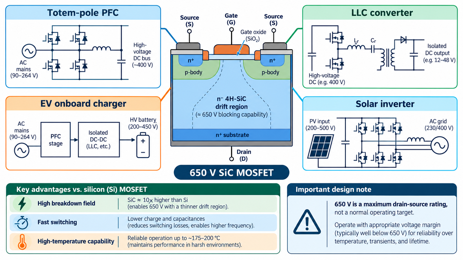
The 650 V number is an absolute maximum rating under specified conditions, not a target operating bus. Designers need margin for line tolerance, switching overshoot, surge, temperature, aging, and reliability requirements.
What silicon carbide changes
Silicon carbide has a wider bandgap and higher critical electric field than silicon. A blocking layer can therefore be thinner and more heavily doped for a given voltage class, supporting low resistance and fast switching. SiC also performs well at elevated junction temperature, although packages, gate oxides, solder, capacitors, magnetics, and cooling still limit the complete system.
The broad application guide at what SiC MOSFETs are used for places 650 V parts among higher-voltage SiC families.
Why 650 V fits a 400 V-class bus
Single-phase rectified mains with PFC often creates a DC link around 380 to 420 V. A 650 V switch provides headroom above that bus, but allowable steady voltage depends on worst-case line, control tolerance, ringing, surge, and standards. Totem-pole PFC, LLC resonant stages, phase-shifted bridges, and selected hard-switched topologies use this class.
Never subtract nominal bus from 650 V and call the remainder safe overshoot. Analyze repetitive and nonrepetitive stress, device derating policy, lifetime, and measurement uncertainty.
Where 650 V SiC MOSFETs are used
Applications include high-efficiency server and telecom supplies, data-center power, solar string and microinverters, energy-storage converters, UPS equipment, industrial auxiliary supplies, EV onboard chargers, charging modules, and high-frequency DC-DC conversion. The value proposition is often smaller magnetics and cooling at high efficiency.
SiC is not automatically optimal at every power. Silicon superjunction MOSFETs can be cost-effective, while GaN may excel in some very-high-frequency 650 V applications. Qualification, supply chain, control, cooling, and system cost decide.
Conduction and switching behavior
Conduction loss depends on hot RDS(on) and RMS current. Switching loss depends on charge, capacitance, voltage, current, gate resistance, driver strength, frequency, reverse conduction, and layout. SiC’s low charge and fast transitions can reduce loss, but also create high dV/dt and di/dt that expose parasitic inductance and capacitance.
The comparison in whether switching a MOSFET reduces heat applies: fast switching lowers some losses but can raise EMI and overshoot if uncontrolled.
Gate drive is device-specific
Use the exact manufacturer’s recommended positive and negative gate voltages. Different SiC generations may specify different drive levels. The driver needs adequate peak current, high common-mode immunity, low propagation mismatch where relevant, local decoupling, and often reinforced isolation. Kelvin-source connections reduce common-source inductance.
Follow how to drive a SiC MOSFET for gate-loop layout, resistance, Miller control, isolation, and measurement. Keep VGS within recommended and absolute limits during every transient.
Reverse conduction and short-circuit protection
A SiC MOSFET can conduct reverse current through its channel when driven on and through its intrinsic diode or third-quadrant behavior when off. Dead time and synchronous timing affect loss. Reverse characteristics differ from silicon, so use device curves and topology-specific measurements rather than assuming a familiar body-diode model.
Short-circuit withstand time may be brief. Fast detection, gate shutdown, desaturation or current sensing, controlled turn-off, and low-inductance protection are essential. Analyze overvoltage created when interrupting fault current.
How to select and validate a 650 V part
Define maximum drain voltage, current waveform, frequency, cooling, ambient, isolation, fault energy, and qualification. Compare maximum hot on-resistance, gate charge, switching energy at relevant conditions, output charge, reverse behavior, package inductance, creepage, thermal impedance, short-circuit data, and reliability documentation. Use vendor models within their stated limits.
The thermal framework in calculating MOSFET heatsink size still applies. Verify VDS, VGS, current, temperature, efficiency, EMI, startup, shutdown, load steps, and faults on the production-intent PCB.
System-level reasons to choose the technology
Evaluate SiC against a credible silicon or GaN baseline at the same output power, cooling, EMI limit, and lifetime. A SiC device may justify its cost through lower semiconductor loss, a higher practical switching frequency, smaller magnetics, a smaller heatsink, or operation at higher coolant temperature. Those savings appear only if the controller, gate driver, transformer, PCB, filter, and mechanical design are optimized with it.
Plan measurement access before layout release. Provide safe locations for high-bandwidth VDS, VGS, current, and temperature measurements without adding long stubs. Define acceptable overshoot and ringing, not just average efficiency. Review common-mode current through isolation capacitance and heatsinks because high dV/dt can create emissions even when the power loop is compact. Finally, verify vendor qualification, traceability, second-source strategy, and production gate-drive tolerances. Wide-bandgap performance is a system achievement, not a drop-in property.
Frequently asked questions
Can a 650 V SiC MOSFET run continuously at 650 V?
No. 650 V is an absolute maximum drain-source rating. Normal operation needs margin for tolerance, ringing, surge, temperature, and reliability.
Is a 650 V SiC MOSFET a direct replacement for silicon?
Usually not. Gate voltage, driver, switching speed, reverse behavior, package, protection, EMI, and thermal design must be reviewed.
Why use SiC on a 400 V bus?
It can reduce switching and high-temperature losses and enable higher frequency, which may shrink magnetics and cooling when the system is designed accordingly.
Does SiC eliminate the need for a heatsink?
No. Lower loss can reduce cooling requirements, but junction temperature still depends on conduction, switching, package, PCB, interface, airflow, and ambient.