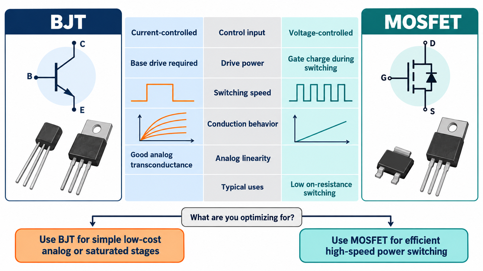
Use a MOSFET when the circuit needs fast, efficient voltage-controlled switching; use a BJT when current-controlled behavior, low cost, linear gain, or a favorable saturation voltage at the target operating point is more important. Neither device is universally better. The correct choice comes from total loss, required drive circuitry, safe operating area, thermal limits, and the way the transistor will be used.
A BJT conducts collector current in proportion to base current and stores minority carriers. A MOSFET controls a channel with gate-to-source voltage and ideally draws almost no steady gate current, although its capacitances must be charged and discharged. That difference shapes almost every practical tradeoff.
Start with the job the transistor must do
Separate switching applications from linear ones. In a switch, the transistor should spend most of its time fully off or fully on. Conduction and transition losses dominate, so a power MOSFET is often the natural choice in converters, motor drives, load switches, and digital interfaces. If the device must amplify a small signal or regulate current while holding a significant voltage, transconductance, bias stability, noise, distortion, and safe operating area matter more. BJTs remain useful in discrete analog stages, current mirrors, low-noise inputs, and some inexpensive high-voltage supplies.
For a refresher on the insulated-gate device, see how a MOSFET transistor works. The operating mode must be decided before comparing headline ratings.
Compare conduction loss at the real current
A MOSFET in hard enhancement is commonly estimated with P = I²RDS(on). Use the resistance at the available gate voltage and expected junction temperature, not only the attractive 25 °C maximum. A BJT near saturation is often estimated with P = VCE(sat)I, but VCE(sat) depends on collector current, forced beta, base drive, and temperature. At low voltage and high current, a very low-resistance MOSFET is usually efficient. At modest current and high voltage, a BJT can remain economically competitive.
Include copper, driver, snubber, and magnetic losses. A cheap transistor that requires a large continuous base current may increase loss elsewhere, while a large MOSFET may demand a strong driver because its total gate charge is high.
Account for switching speed and drive power
A BJT must remove stored charge before it can turn off, especially after deep saturation. That makes high-frequency switching harder and can increase crossover loss. A MOSFET has no minority-carrier storage in the channel, but its gate charge, Miller plateau, output capacitance, and common-source inductance still limit transition speed. Driver peak current is approximately the charge that must move within the desired switching interval; average gate-drive power rises with gate charge, drive voltage, and frequency.
The practical guidance in tuning a MOSFET gate resistor shows why the fastest edge is not automatically the best edge. EMI, overshoot, and false turn-on may require controlled switching.
Examine control, gain, and linearity
BJTs offer high transconductance per unit bias current, which is valuable in analog gain stages. Their base-emitter voltage and current gain vary with temperature and device spread, so bias networks need feedback or degeneration. MOSFET gates simplify DC drive, but threshold voltage is not a precision turn-on voltage and varies widely. In a linear MOSFET amplifier, the selected device must have a suitable DC safe operating area; a switching-optimized MOSFET can suffer localized heating when it holds high voltage and current simultaneously.
Audio and RF circuits may use either technology, sometimes in complementary roles. The decision should be based on noise, input impedance, gain, distortion, capacitance, bandwidth, and thermal tracking rather than the label on the package.
Check voltage stress and safe operating area
Absolute maximum voltage is a boundary, not a design target. Add margin for supply tolerance, inductive overshoot, load dump, transformer leakage, and ringing. A MOSFET also has gate-oxide limits and may need a clamp. A BJT needs adequate reverse base-emitter protection and must avoid second breakdown. Read the safe-operating-area graph at the actual pulse width and case temperature; a current rating printed on the first page rarely describes the usable high-voltage operating point.
The related article on why MOSFETs get hot explains how electrical stress becomes junction temperature and why pulsed ratings require careful interpretation.
Evaluate temperature and parallel operation
MOSFET on-resistance normally rises with temperature, which helps steady-state current sharing among well-matched parallel devices. Dynamic sharing can still be poor when gate loops or power paths differ. BJT collector current can increase as temperature raises gain or lowers the required base-emitter voltage, so emitter resistors and thermal coupling are often required to prevent current hogging. Neither technology should be paralleled casually.
Calculate loss at the hottest credible junction, build the junction-to-ambient thermal network, and measure the assembled product. Cooling, package choice, PCB copper, airflow, and mounting pressure can outweigh a small electrical advantage in the transistor itself.
Use a disciplined selection process
Write down maximum voltage, RMS and peak current, duty cycle, frequency, ambient temperature, cooling, available drive voltage and current, fault duration, and lifetime target. Shortlist devices, then calculate worst-case conduction, switching, and drive losses. Check startup, current limit, short circuit, and inductive turn-off. Simulate parasitics, but validate with a current-limited prototype and properly rated probes.
If the result points to a MOSFET, follow the connection practices in how to wire a MOSFET. A good device selected without a low-inductance gate loop, return path, clamp, and thermal path can perform worse than a theoretically inferior device used correctly.
Frequently asked questions
Is a MOSFET always more efficient than a BJT?
No. MOSFETs often win at high switching frequency, but efficiency depends on current, voltage, on-resistance, switching charge, drive loss, and temperature. A BJT can be competitive in a low-frequency, low-power, high-voltage design.
Can I replace a BJT with a MOSFET directly?
Usually not. The drive polarity, required voltage or current, pinout, bias network, switching behavior, and protection differ. Redesign and verify the surrounding circuit.
Which device is better for an amplifier?
It depends on noise, gain, input impedance, distortion, power, bandwidth, and bias stability. Both BJT and MOSFET amplifiers can be excellent when designed around their device characteristics.
Which is easier to drive from a microcontroller?
A small logic-level MOSFET may be convenient, but high current or high frequency normally requires a dedicated gate driver. A BJT needs controlled base current and often a resistor or driver stage.