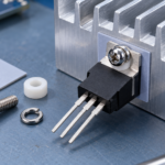
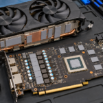
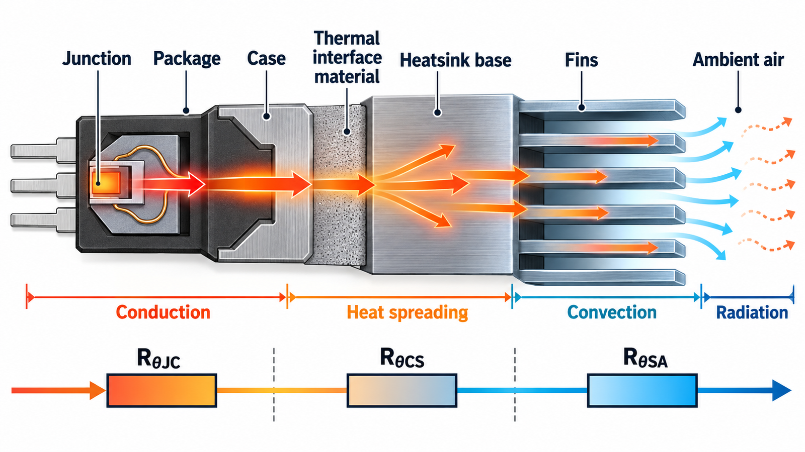
A heatsink cools a MOSFET by providing a low-resistance path from the hot semiconductor junction to a large metal surface, where air carries the heat away. Heat first crosses the package, then a thermal interface, spreads through the heatsink base, and reaches the fins. Natural convection or a fan replaces warmed air with cooler air.
The heatsink does not force the MOSFET to ambient temperature. Every watt flowing through the thermal path creates a temperature rise. Successful cooling therefore begins with realistic power-loss calculations and ends with measurement on the assembled product.
The thermal-resistance chain
The common steady-state model is junction-to-case resistance RθJC, case-to-sink resistance RθCS, and sink-to-ambient resistance RθSA. A first estimate is TJ = TA + P(RθJC + RθCS + RθSA). This simple chain assumes all relevant heat takes that path and conditions match the ratings.
Board-mounted packages also send heat into copper and vias. Nearby parts warm the local air and sink. For a worked sizing method, see how to calculate heatsink size for a MOSFET.
Why fins and airflow matter
A flat metal plate spreads heat, but fins add surface area without requiring a huge footprint. More surface allows more convection, provided air can reach it. In natural convection, warm air rises through vertical channels. Horizontal or blocked fins perform worse. With forced air, fin pitch, ducting, fan pressure, inlet temperature, filters, and downstream heating determine performance.
Published RθSA values apply to stated conditions. A small fan in open air may deliver far less flow after a grille, filter, and dense fins are added. Dust accumulation and fan wear must be included in lifetime margin.
The interface fills microscopic gaps
Package and heatsink surfaces look flat but touch at small high points. Air in the remaining voids conducts heat poorly. A thin layer of thermal compound, pad, phase-change material, or approved insulator fills those voids. The best choice balances thermal resistance, electrical isolation, thickness tolerance, pump-out, aging, cleanliness, and manufacturing repeatability.
More compound is not better. Excess thickness adds resistance. If a MOSFET tab is electrically connected to the drain, an insulating pad and shoulder washer may be necessary. The guide to sharing a heatsink among MOSFETs explains the electrical hazard.
Mounting pressure changes performance
Correct pressure squeezes the interface into a controlled bond line and maintains contact during thermal cycling. Too little pressure leaves gaps; too much can crack the package, bow the heatsink, extrude a pad, strip threads, or puncture insulation. Follow the package and interface supplier’s torque or clip-force guidance. Deburr holes and keep metal particles away from the pad.
A spring clip can maintain more consistent force than a screw, but geometry matters. After assembly, inspect pad coverage and verify electrical isolation where required. A visually tight screw does not prove a good thermal joint.
The heatsink must remove actual MOSFET loss
Conduction loss is approximately I2RDS(on) and rises as resistance increases with temperature. Switching loss depends on voltage, current, transition time, frequency, driver strength, capacitances, reverse recovery, and parasitic inductance. Linear operation or avalanche can create concentrated heating not captured by a simple average-current estimate.
Read why MOSFETs get hot before selecting RθSA. Oversizing the heatsink cannot always rescue a device operated outside its safe operating area, because heat may localize inside the die faster than the package can spread it.
How to verify the cooling design
Calculate worst-case loss at maximum current, voltage, switching frequency, hot RDS(on), maximum ambient, and minimum airflow. Include interface and spreading resistance. Prototype with a current-limited source and measure temperatures after thermal equilibrium and during relevant transients. A thermocouple, calibrated thermal camera, or temperature-sensitive electrical parameter can be used with care.
The PCB is often part of the heatsink; designing the PCB thermal path covers copper planes and vias. Validate blocked vents, failed fans, orientation, enclosure heating, and neighboring loads. Keep operating junction temperature below the absolute maximum with reliability margin.
A practical cooling review
Before freezing the mechanical design, review the assembly from the junction outward. Confirm the loss model uses hot electrical values, the package thermal metric matches the heat path, the interface is compatible with the voltage and mounting pressure, and the heatsink rating matches its orientation and airflow. Check whether another component warms the inlet air or baseplate. Confirm that the enclosure gives hot air somewhere to leave.
Then review manufacturability. Specify surface flatness, cleanliness, interface thickness, screw torque or clip force, insulation test, fan connector, and inspection criteria. Record thermocouple or thermal-camera locations so production samples are measured consistently. A useful design margin covers fan tolerance, dust, aging, high ambient, and unit-to-unit power spread. If the MOSFET temperature estimate changes dramatically with a small assumption, improve the model or the thermal path rather than relying on a single optimistic calculation.
Frequently asked questions
Does a bigger heatsink always cool better?
Usually a larger effective area helps, but poor airflow, a thick interface, a thin base, wrong fin orientation, or bad contact can dominate. Compare thermal resistance under the real conditions.
Can a heatsink make a MOSFET colder than ambient?
No, not by passive cooling alone. A passive sink moves heat toward ambient; thermoelectric or refrigeration systems are needed to go below ambient.
Do all MOSFETs need a heatsink?
No. Low-loss devices may be cooled by package leads and PCB copper. The decision follows calculated and measured junction temperature.
Why is my heatsink cool while the MOSFET fails?
The interface may be poor, the heat pulse may be too fast, the die may be in an unsafe linear region, or measurement may miss a local hotspot.